Chinese semiconductor industry

Status
Not open for further replies.

tokenanalyst

Brigadier
Registered Member

CAS Microelectronics has made important progress in hafnium oxide-based ferroelectric storage materials.​

The rapid development of information technologies such as the Internet and artificial intelligence has put forward higher requirements for the storage density, access speed and number of operations of the memory. Hafnium oxide-based ferroelectric memory has the advantages of low power consumption, high speed, and high reliability, and is considered as a potential solution for the next generation of non-volatile memory technology. Orthorhombic phase (orthorhombic phase , referred to as "o phase " ) HfO 2 -based ferroelectric materials that are widely studied now, due to their own high ferroelectric flipping potential barrier and " independent flipping " dipole flipping mode, devices based on this ferroelectric material It has a high coercive field, which leads to problems such as the incompatibility of the operating voltage of the device with the advanced technology node, and the limited number of erasing and writing times. This problem is based on the intrinsic properties of o -phase HfO2 - based ferroelectric materials, which is difficult to solve by conventional optimization processes. Therefore, finding a HfO2 - based ferroelectric material with stable structure and low flipping barrier is an urgent problem to be solved.

  In response to this problem, the team of academician Liu Ming of the Key Laboratory of Microelectronic Devices and Integrated Technology and the team of researcher Du Shixuan of the Institute of Physics, Chinese Academy of Sciences discovered a stable ferroelectric trigonal phase Hf(Zr) 1+x O 2 material structure , This structure lowers the flipping barrier of ferroelectric dipoles in HfO2 - based ferroelectric materials. Through first-principle calculations based on density functional theory ( DFT ), it is found that when the ratio of Hf(Zr) to oxygen in Hf(Zr) 1 + x O 2 material is greater than 1.079 : 2 , the formation energy of the trigonal phase is low In the formation energy of ferroelectric o- phase and monoclinic phase ( m -phase). Scanning transmission electron microscopy ( STEM ) experiments clearly revealed the crystal structure of excess Hf(Zr) atoms embedded in the ferroelectric trigonal lattice, confirming the results of theoretical calculations. The embedded Hf(Zr) atoms expand the lattice, increase its in-plane and out-of-plane stresses, and play a role in stabilizing the structure of Hf(Zr) 1+x O 2 materials and lowering their ferroelectric flipping barrier. Based on Hf(Zr) 1+x O2 Thin-film ferroelectric devices exhibit ultra-low coercive field (0.65MV /cm ), high remanent polarization ( P r ) value (22μC/cm 2 ) , small saturation polarization electric field ( 1.25MV/cm ) , and a large breakdown electric field ( 4.16MV/cm ), and achieved a durability of 10 12 cycles under saturated polarization. The findings provide an effective solution for low-power, low-cost, long-life memory chips.
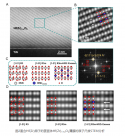
1692716616160.png
Please, Log in or Register to view URLs content!
 

Hendrik_2000

Lieutenant General
The link was provided by Vincent. Well, the light source is the only bottleneck then. I agree with the prof the difficulty is creating a complete domestic supply like for lithograph machines But it will come just like Gas turbines, Space technology, Solar panels, etc. It just takes time
Please, Log in or Register to view URLs content!

Zhu Yu from Tsinghua University: The research group’s development of the workpiece table is at the same level as ASML in a large generation​

Author:
Please, Log in or Register to view URLs content!
08-21 16:45
mes-icon.png
评论
sc-icon.png
收藏
zan-icon.png
点赞
Source: Aijiwei #lithography# #Qinghua# #Workpiece table#
7043
node-list-look.png

According to news from Weibo, Tsinghua University’s Department of Mechanical Engineering’s official Wechat platform, The Voice of Machinery, recently published an article introducing the Manufacturing Frontier Lecture held by the department on August 13 – a special event on integrated circuits.

This event invited the Department of Mechanical Engineering of Tsinghua University Long-term professor Zhu Yu gave a special lecture on lithography machine technology.
According to Professor Zhu Yu, a number of research institutes in my country are working together on DUV lithography machine research and EUV lithography machine key technology pre-research. Research and development of engraving machines, vacuum workbenches, etc.

Subsequently, Chai Zhimin, an assistant professor and researcher at the Department of Mechanical Engineering of Tsinghua University, gave a lecture on chip technology and shared several cutting-edge patterning technologies currently being studied in my country in the field of lithography, such as near-field lithography technology, nanoimprint technology, Copolymer directed self-assembly lithography, etc.

In the free communication session of the activity, some students asked Zhu Yu about the gap between the workpiece table developed by his research group and ASML company. Zhu Yu responded that: the work table developed by the research group is at the same level as the most advanced work table (products above 2000 series) of ASML in a large generation. However, there is still a generation gap with ASML's 2000 series and above products in a small generation, and it can catch up with the international advanced level after one more iteration.

In response to the question that my country's research and development of lithography machines has been sanctioned in terms of various components, Zhu Yu said that ASML's lithography machines are made based on the global supply chain. China needs to cultivate its own suppliers and build its own supply chain. The difficulty is far greater than the research and development process in other countries. I believe that in the near future, China will overcome all technical difficulties.
 

tphuang

Lieutenant General
Staff member
Super Moderator
VIP Professional
Registered Member

CAS Microelectronics has made progress in the field of 28nm RRAM in-memory computing circuits​

The rapid development of the Internet of Things and artificial intelligence technology has put forward higher requirements for the real-time data processing capability and energy efficiency of the edge node computing platform. The non-volatile in-memory computing technology based on the new memory can realize the in-situ storage and calculation of data, and minimize the power consumption and delay overhead caused by data transfer, thereby greatly improving the data processing capability and performance ratio of edge devices. However, non-volatile in-memory computing still faces limitations in computing performance and energy efficiency due to non-ideal factors in the characteristics of the basic unit, parasitic effects in the array, and the hardware overhead of the analog-to-digital conversion circuit.
  Focusing on the above key issues, the team of academician Liu Ming of the Institute of Microelectronics adopted a cross-level collaborative design method to propose a new RRAM in-memory computing structure with high parallelism and high performance ratio.
  At the device level, the research team proposed a memory-computing array structure with a weighted two-transistor-memristor ( WH-2T1R ). The WH-2T1R structure uses core transistors to form a decoupled storage and calculation data path to reduce the impact of parasitic effects on the calculation current. Compared with the 1T1R structure, it only causes an additional 30.3% area overhead. The calculation unit utilizes the amplification characteristics of the second transistor sub-threshold region to increase the calculation switching ratio by 13.5 times while reducing the calculation current in the low-resistance state by 88% , thereby achieving a 63.4% reduction in the power consumption of the multiply-add operation. Thanks to the improvement of the calculation switch ratio, the RRAM memory calculation structure can support higher input parallelism and multi-bit multiplication and addition operations.
  At the circuit level, the research team proposed a readout circuit for a reference current subtraction current-type sense amplifier. The reference current subtraction branch first subtracts the input current according to the last readout result and then sends it to the current mirror to read out the data. The reference current subtraction branch reduces the input current range of the current mirror in half, doubles the calculation current range supported by the RRAM storage and calculation structure, and can achieve higher input parallelism and multi-bit multiplication and addition, and achieve 79.5% of the power consumption of the readout circuit reduce. By further optimizing the current subtraction configuration of the current-type sensitive amplifier, the research team achieved a 5 -fold increase in the integral nonlinear error and a 3.75 -fold increase in the differential nonlinear error .
  At the level of algorithm mapping, the research team proposed a high data redundancy ( MSB_RSM ) mapping strategy. The RRAM in-memory computing structure is equipped with multiple sets of arrays with different second transistor multiplier parameters and an additional set of redundant arrays. Wherein different second transistors are used to map different bits of the multi-bit weight value. Since the impact of RRAM and transistor non-ideal factors on the calculation current cannot be ignored, redundant arrays are used for additional mapping weights to compensate for non-ideal factors. After analyzing the compensation effects of different bits, MSB-RSM can reduce the 1σ error by 40% when operating on high-bit weights . Thanks to the more stable calculation current, the CIFAR-10 and CIFAR-100 tasks under the ResNet-18 model have achieved 0.96% and 2.83% accuracy improvements.
  The above scheme has been verified on the embedded 28nm process independently developed by the team . The new RRAM in-memory computing structure supports highly parallel analog domain multiplication and addition operations. In the ResNet-18 task with 1 -bit input, 3 -bit weight, and 4- bit output The average energy efficiency reaches 30.34TOPS/W , and can be increased to 154.04TOPS/W by further optimizing the readout timing . This work provides a new idea for high-energy-efficiency, high-precision analog in-memory computing through the system design of units, circuits, and systems.


View attachment 117524

Please, Log in or Register to view URLs content!
This is important I think. I wonder where smic is with this? Wasn't tsmc already doing 22nm rram on their MCUs?
 

HereToSeePics

Junior Member
Staff member
Moderator - World Affairs
Registered Member
So basically the US knows it cannot stop the progress of Chinese AI, but basically make China buy twice as many nVidia chips.
Good for shareholders, lol

Maybe someone should let
Please, Log in or Register to view URLs content!
know that every pound of CO2 reduction from US green energy projects will be offset by the extra coal power stations China will be building to power data centers using these less efficient chips
 

supersnoop

Major
Registered Member
Maybe someone should let
Please, Log in or Register to view URLs content!
know that every pound of CO2 reduction from US green energy projects will be offset by the extra coal power stations China will be building to power data centers using these less efficient chips

They are counting on China being the leaders in Green Energy

I hate polluting (pun intended) threads, but the coal thing really gets my goat
So on one hand, we have these stories in Mainstream media
Please, Log in or Register to view URLs content!

What most people won't actually read is that many plants are approved but not actually built
Please, Log in or Register to view URLs content!
 

HereToSeePics

Junior Member
Staff member
Moderator - World Affairs
Registered Member
They are counting on China being the leaders in Green Energy

I hate polluting (pun intended) threads, but the coal thing really gets my goat
So on one hand, we have these stories in Mainstream media
Please, Log in or Register to view URLs content!

What most people won't actually read is that many plants are approved but not actually built
Please, Log in or Register to view URLs content!

Yep, I get that China has been leading on green energy and zero carbon energy infrastructure, but there's no harm in pitting the climate change pundits and the semiconductor/economic warfare interests against each other since the US is essentially forcing China's hand on using more energy wasteful processes.
 

tphuang

Lieutenant General
Staff member
Super Moderator
VIP Professional
Registered Member
Interesting
Please, Log in or Register to view URLs content!

So basically the US knows it cannot stop the progress of Chinese AI, but basically make China buy twice as many nVidia chips.
Good for shareholders, lol
I would advise that you stop believing in what these articles are saying. Chip to chip transfer speed is a small part of GPU computation cluster.

And stop using statements like making china buy twice as many Nvidia chips. Chinese operators are buying Nvidia chips because they are buying chips from everyone domestic and abroad.

This is something I have been trying to explain for a while. People outside china simply has no clue the amount of computational expansion and llm demand in china right now. At some point, Chinese firms will not longer need Nvidia chips, but we are not there yet.
 

supersnoop

Major
Registered Member
I would advise that you stop believing in what these articles are saying. Chip to chip transfer speed is a small part of GPU computation cluster.

And stop using statements like making china buy twice as many Nvidia chips. Chinese operators are buying Nvidia chips because they are buying chips from everyone domestic and abroad.

This is something I have been trying to explain for a while. People outside china simply has no clue the amount of computational expansion and llm demand in china right now. At some point, Chinese firms will not longer need Nvidia chips, but we are not there yet.

Well, I think it's a good time to explain to a neophyte what this actually means.
My assumption was that chip to chip transfer speed is important when down data sets are broken down to be analyzed in parallel.
If this the Chinese version is running at 60% of this speed, then conversely you could make up for it with more chips.

They are also buying nVidia chips because the article says the price performance ratio is still good. It is also routinely discussed here and elsewhere that CUDA is well established and there exists a large talent pool for it.

There is no shame in buying or needing nVidia chips at the moment. nVidia has been around for decades, I wouldn't expect there to be big Chinese competition all of a sudden. Heck, why is AMD so behind nVidia in this department even?
 
Status
Not open for further replies.
Top