Chinese semiconductor industry

Status
Not open for further replies.

olalavn

Senior Member
Registered Member
Innosilicon "Fenghua 2" is a 4K-level high-performance strong rendering four-screen desktop and embedded GPU, using a full set of self-developed high-end IP, with intelligent computing capabilities, ultra-low power consumption, strong performance, strong rendering , high security, multi-screen display, high adaptability, multi-platform, high bandwidth and other eight innovative advantages.

Fully supports domestic and foreign CPU/OS ecology, including Linux, Windows (including DX11) and Android


Please, Log in or Register to view URLs content!
 

tokenanalyst

Brigadier
Registered Member

Jiaxin Semiconductor, a subsidiary of Wanye Enterprise, signed a strategic cooperation agreement with Jiashan Fudan Research Institute​

On August 16, Jiaxin Semiconductor Equipment Technology Co., Ltd. (hereinafter referred to as "Jiaxin Semiconductor"), a holding subsidiary of Wanye Enterprise, announced a strategic cooperation with Jiashan Fudan Research Institute. Ding Shijin, vice president of Jiashan Fudan Research Institute, and Zhou Weifang, chairman and CEO of Jiaxin Semiconductor Equipment Technology Co., Ltd., attended the strategic signing ceremony.
According to the content of the strategic cooperation agreement, the two parties will uphold the principles of "mutual benefit and win-win, openness and fairness, voluntary equality, and complementary advantages" to establish a strategic partnership and work together on scientific research cooperation, industrial cooperation, and talent exchanges in the field of integrated circuits. Form a long-term and stable cooperative relationship, give full play to their respective resource advantages, and achieve the strategic goal of common development. The focus of cooperation will focus on three aspects of scientific and technological cooperation, industrial cooperation and talent exchange, and carry out all-round mutually beneficial cooperation in the fields of technological breakthroughs, innovation platform project declaration, transformation and promotion of scientific and technological achievements, open sharing of R&D resources and services, and deep integration of industry-university-research. , in order to promote the development of high-quality "chips" of integrated circuits in Zhejiang and Jiashan.
From the perspective of overall strength, the strategic partners have long-term experience and technology accumulation in their respective fields, and have extensive advantages integration and complementary cooperation foundation. Jiaxin Semiconductor, as one of the cutting-edge local semiconductor core equipment companies, was established in April 2021 by Wanye Enterprise, a listed semiconductor equipment company, and world-renowned industry experts. The total investment scale is 2 billion yuan, and the land area is 109 acres. And the key equipment for manufacturing etching, thin film deposition, rapid heat treatment and other mature integrated circuit processes. The product range covers many important categories of chip manufacturing core equipment. Since the second half of 2022, Jiaxin Semiconductor has won bids for customer-specific process production lines many times, including silicon nitride plasma etching machines, metal plasma etching machines, deep groove etching machines, and side wall plasma etching machines; high-density plasma thin films Deposition equipment (HDP-CVD), doped boron phosphorus silicon dioxide film chemical deposition equipment (SACVD), titanium/titanium nitride deposition equipment (MOCVD), aluminum copper metal sputtering equipment (metal Sputter (Al/Ti/ TiN )); rapid thermal treatment (RTP) equipment and multiple types of equipment such as double combustion + double water washing tail gas treatment.

Jiashan Fudan Research Institute is a key laboratory built to respond to and implement the national strategy of the "Yangtze River Delta Integrated Development Plan". Relying on the academic advantages of Fudan University's integrated circuit industry chain, the research institute is committed to the construction of high-level innovation carriers, scientific research and achievement transformation, empowering local industry upgrading, creating a collaborative innovation ecology, and assisting digital reform. As the first round of key construction of the Zhejiang branch of the National Integrated Circuit Innovation Center, the Institute is responsible for the "bridgehead" of Fudan University's human resources, innovation resources, industrial resources and Zhejiang's regional characteristic economy, and promotes the construction of an integrated collaborative innovation industry system in the Yangtze River Delta. .

Please, Log in or Register to view URLs content!
 

tokenanalyst

Brigadier
Registered Member

Jingce Electronics: The front-line measurement breaker bravely enters the domestic alternative deep-water area​


  Through independent research and development and incubation, the company has expanded from panel testing to semiconductor front-end measurement.

  The company started in the field of panel inspection, and continued to improve its layout in the field of flat panel inspection 19 years ago. It expanded from AOI optics and module inspection to high-value OLED inspection and other fields. Since 20 years, it has gradually entered the field of semiconductor front-end measurement equipment. Domestic products replace deep-water areas, and the products cover core mainstream products such as film thickness, OCD, electron beam, and bright field.

  The front-end measurement and testing of semiconductors is getting better and better, breaking the overseas monopoly and achieving breakthroughs in shortcomings. Semiconductor front-end inspection and measurement equipment accounts for 11% of the value of semiconductor equipment. In 22 years, China's inspection and measurement equipment market space was 3.1 billion US dollars, and the localization rate was less than 10%. Most of the market was monopolized by overseas companies such as KLA. The company continues to aim at this track to achieve domestic breakthroughs. According to the company's annual report, the company's semiconductor field orders in hand in 22 years are about 900 million yuan, which is about 5 times the operating income of the business that year. The products that have been developed and verified are expected to support future continued growth.

  This year, the company disclosed two major contracts for front-end measurement and testing, becoming a breaker for domestic substitution.

  High market recognition. In April, Shanghai Jingce, a holding subsidiary, signed an order of 120 million for multiple semiconductor front-end measurement and testing equipment with customers. In August, Shenzhen Jingjiwei, a holding subsidiary, signed a 170 million order for semiconductor front-end inspection Equipment orders. At the current stage, domestic front-end measurement and testing equipment has been deployed in domestic deep-water areas, and customer orders and verification are the key to breakthroughs in the next step.

  Display panel testing equipment is leading in China, and it is developing into new fields such as Micro+ and VR/AR. The company has a relatively high market share in the field of domestic display panel testing; on this basis, the company has raised investment projects for many times and established subsidiaries to expand in new fields such as AR/VR and Micro-OLED. In 22 years, some of the company's products have gained international Batch orders from well-known top customers and partial delivery completed.​
 

tokenanalyst

Brigadier
Registered Member

Jingce Electronics: Signing semiconductor testing sales contracts continues to benefit from domestic substitution​


Subsidiary signed a contract, and Qiandao Semiconductor became a new growth point for performance. Shenzhen Jingji Micro was established in early 2023, with Jingce Electronics holding 37.5% of the shares and Shanghai Jingji Micro holding 62.5% of the shares. The main business is semiconductor testing The R & D and production of equipment will help to enhance the company's comprehensive competitiveness and further expand the company's customer resources. On August 11, 2023, Shenzhen Jingji Micro signed a sales contract with the customer, planning to sell semiconductor front-end testing equipment to the customer, with a transaction amount of 173 million. The signing of the contract is a further deepening of the cooperative relationship between the company and the customer on the basis of good cooperation, which reflects the customer's high recognition of the company's semiconductor testing equipment, and helps to expand the company's brand influence and enhance the company's market competitiveness. The company continues to benefit from the domestic substitution of semiconductor testing equipment, and is expected to occupy a broader domestic market in the future. The semiconductor testing business has become an important engine for the company's performance growth.

The front/back-end semiconductor testing has a layout, and the technical barriers are deep. In the field of semiconductor testing, the company is a leading enterprise in China that covers both front/back-end semiconductor testing equipment. In 2022, the company's semiconductor sector will achieve sales revenue of 183 million yuan, a year-on-year increase of 34.12% over the same period in 2021. As of April 2023, the company's orders in hand in the semiconductor field are about 891 million yuan.

The front-end detection link mainly relies on Shanghai Jingce. The film thickness measurement equipment and electron beam defect detection equipment have obtained batch orders from domestic first-line customers; OCD equipment has passed the verification of many first-line customers and has obtained some orders; bright field optics Defect detection has extremely high technical barriers. The company has won two orders for bright field detection equipment and completed the delivery of the first one. The back-end link mainly relies on Wuhan Jinghong. The Burn-In product line has achieved repeated orders in batches from domestic first-line customers, and the related products of the CP/FT product line have obtained corresponding orders and completed delivery.
 

tokenanalyst

Brigadier
Registered Member

Semiconductor Advanced Ceramic Materials Research Institute settled in Jiangsu Taixing High-tech Zone​


According to Taizhou Science and Technology News, on August 11, the Jiangsu Industrial Technology Research Institute/Yangtze River Delta National Technology Innovation Center Semiconductor Advanced Ceramic Materials Research Institute was officially unveiled and settled in Jiangsu Taixing High-tech Zone.

It is understood that the Institute of Semiconductor Advanced Ceramic Materials was jointly established by Taixing High-tech Zone, Jiangsu Industry and Research Institute/Yangtze River Delta National Innovation Center, Taizhou Industry and Research Institute and Professor Pan Wei of Tsinghua University, with the goal of cultivating and developing semiconductor materials and equipment parts industries , focusing on breakthroughs in the commonality and key technologies of the semiconductor ceramic material industry, carry out industrial technology application research and integrated innovation, promote the transfer and transformation of scientific and technological achievements, derive and incubate technology-based enterprises, cultivate high-level innovative talents, and strive to create international-level semiconductor ceramic materials Technology research and development center and industrial base.

According to the data, the Institute of Semiconductor Advanced Ceramic Materials relies on the State Key Laboratory of New Ceramics and Fine Technology of Tsinghua University. It has core products and patented technologies such as high thermal conductivity ceramic substrates and precision ceramic components for semiconductor equipment. It is at the world's advanced level and can meet market requirements. Rigid demand for domestic substitution of advanced ceramic components. The institute will focus on semiconductor key ceramic components, high thermal conductivity ceramic substrates, semiconductor ceramic powders, etc., to build a public technical service platform for powder research and development, process molding, sintering, and performance testing of semiconductor advanced ceramic materials, and to carry out industrial common and key research and development. Technology research and development, as well as the development and optimization of new technological processes for ceramic preparation.

Please, Log in or Register to view URLs content!
 

tokenanalyst

Brigadier
Registered Member

Keystone signed a new customer order for 12-inch wafer fab​


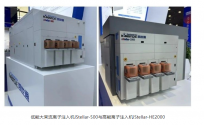
As a leader in the industrialization of domestically produced low-energy, large-beam and high-energy ion implanters, Kaistone has signed purchase orders with a number of mainstream customers of 12-inch integrated circuit manufacturing plants since 2020, with a cumulative amount of over 1 billion yuan.

It is reported that the iStellar-500 series of low-energy and large-beam ion implanters adopts the "universal platform + key technology module" research and development model, rapidly iteratively upgrades and expands the product line of ion implanters, covering the needs of different chips for ion implantation, and is positioned to provide customers with Products with higher reliability and lower cost of ownership, and have good production line process matching capabilities and extensive process coverage capabilities. Another high-energy ion implanter equipment, iStellar-HE2000, adopts key technologies such as high-pressure acceleration, high injection angle accuracy, and nano-scale particle pollution control to meet the needs of high-energy ion implantation in chip manufacturing.

1692282124775.png
Please, Log in or Register to view URLs content!
 

tokenanalyst

Brigadier
Registered Member

The new issue of "Acta Optics Sinica" published an invited review, revealing the progress of optical design of my country's EUV lithography objective lens system​


Collecting micro-net news, the authoritative journal in the field of optics in China, "Acta Optics Sinica", Volume 43, Issue 15 (Online Publishing 2023-08-15), published an invited review titled "Research and Progress in Optical Design of Exposure System for Extreme Ultraviolet Lithography Machines" Li Yanqiu's team from the Key Laboratory of Optoelectronic Imaging Technology and Systems of the Ministry of Education of the School of Optoelectronics, Beijing Institute of Technology reviewed the relevant scientific research progress at home and abroad.
According to the article, in 2002, the Changchun Institute of Optics, Fine Mechanics and Physics of the Chinese Academy of Sciences developed the first domestic EUV lithography experimental device composed of a small field of view Schwarzschild objective lens, which realized the exposure of a feature size of 0.75 μm. In 2017, the Changchun Institute of Optics, Fine Mechanics and Physics of the Chinese Academy of Sciences reported that it developed a small field of view EUV exposure optical system. The RMS value of the projection objective lens composed of two mirrors is better than 0.75nm, and a static exposure device for EUV lithography was constructed. , obtained a photoresist exposure pattern with a line width of 32nm, and established a key technology verification and process testing platform for EUV lithography.
In terms of the design of the EUV objective lens system, this article evaluates the domestic research on the design of the uniform magnification EUV lithography objective lens system. At present, the optical design of the objective lens system has reached the international advanced level. The optical design of variable magnification lithography objective lens is in the stage of in-depth research at home and abroad. Beijing Institute of Technology and Changchun Institute of Optics, Fine Mechanics and Physics, Chinese Academy of Sciences have conducted long-term in-depth research on the optical design of EUV exposure systems with NA 0.33 and NA 0.55, and the design method and design effect are comparable to similar designs that have been disclosed internationally.
According to the summary, the current domestic research focuses on the design of objective lens system and lighting system, tolerance analysis, thermal deformation analysis of exposure system and its control research. Beijing Institute of Technology and Changchun Institute of Optics, Fine Mechanics and Physics, Chinese Academy of Sciences have long been engaged in high-performance EUV The design research, design method and design effect of the lithography objective lens and lighting system are at a similar level to similar designs disclosed internationally, which has laid a good foundation for the development of my country's EUV lithography machine and cultivated a large number of talents.

Please, Log in or Register to view URLs content!
 

Hendrik_2000

Lieutenant General
Well progress is being made in the lower segment of semiconductor equipment
Please, Log in or Register to view URLs content!

China to make steady progress in chip equipment self-sufficiency amid gradual market recovery, UBS survey finds
South China Morning Post
Wed, August 16, 2023 at 4:30 AM CDT·3 min read
36

China's chip equipment self-sufficiency rate will keep increasing in the next few years, especially in the less-advanced equipment sector, amid a gradual market recovery and ongoing geopolitical tensions, according to research by UBS Securities.

The semiconductor equipment self-sufficiency rate is expected to increase in less-advanced sectors which account for around 70 per cent of the total market, such as etching and cleaning machines, Jimmy Yu, a China technology analyst at UBS Securities, said at a media briefing in Shanghai on Wednesday.

"You cannot assume that domestic companies will take up 100 per cent of the [Chinese] market, but it is reasonable to make the assumption of a market share of around 60 per cent [in some sectors]," said Yu.

Do you have questions about the biggest topics and trends from around the world? Get the answers with SCMP Knowledge, our new platform of curated content with explainers, FAQs, analyses and infographics brought to you by our award-winning team.
 

ZeEa5KPul

Colonel
Registered Member

The new issue of "Acta Optics Sinica" published an invited review, revealing the progress of optical design of my country's EUV lithography objective lens system​


Collecting micro-net news, the authoritative journal in the field of optics in China, "Acta Optics Sinica", Volume 43, Issue 15 (Online Publishing 2023-08-15), published an invited review titled "Research and Progress in Optical Design of Exposure System for Extreme Ultraviolet Lithography Machines" Li Yanqiu's team from the Key Laboratory of Optoelectronic Imaging Technology and Systems of the Ministry of Education of the School of Optoelectronics, Beijing Institute of Technology reviewed the relevant scientific research progress at home and abroad.
According to the article, in 2002, the Changchun Institute of Optics, Fine Mechanics and Physics of the Chinese Academy of Sciences developed the first domestic EUV lithography experimental device composed of a small field of view Schwarzschild objective lens, which realized the exposure of a feature size of 0.75 μm. In 2017, the Changchun Institute of Optics, Fine Mechanics and Physics of the Chinese Academy of Sciences reported that it developed a small field of view EUV exposure optical system. The RMS value of the projection objective lens composed of two mirrors is better than 0.75nm, and a static exposure device for EUV lithography was constructed. , obtained a photoresist exposure pattern with a line width of 32nm, and established a key technology verification and process testing platform for EUV lithography.
In terms of the design of the EUV objective lens system, this article evaluates the domestic research on the design of the uniform magnification EUV lithography objective lens system. At present, the optical design of the objective lens system has reached the international advanced level. The optical design of variable magnification lithography objective lens is in the stage of in-depth research at home and abroad. Beijing Institute of Technology and Changchun Institute of Optics, Fine Mechanics and Physics, Chinese Academy of Sciences have conducted long-term in-depth research on the optical design of EUV exposure systems with NA 0.33 and NA 0.55, and the design method and design effect are comparable to similar designs that have been disclosed internationally.
According to the summary, the current domestic research focuses on the design of objective lens system and lighting system, tolerance analysis, thermal deformation analysis of exposure system and its control research. Beijing Institute of Technology and Changchun Institute of Optics, Fine Mechanics and Physics, Chinese Academy of Sciences have long been engaged in high-performance EUV The design research, design method and design effect of the lithography objective lens and lighting system are at a similar level to similar designs disclosed internationally, which has laid a good foundation for the development of my country's EUV lithography machine and cultivated a large number of talents.

Please, Log in or Register to view URLs content!
Very interesting and encouraging that China can design NA 0.55 EUV mirrors. Hopefully we'll get some news on where they are with fabrication.
 
Status
Not open for further replies.
Top