You are using an out of date browser. It may not display this or other websites correctly.
You should upgrade or use an alternative browser.
You should upgrade or use an alternative browser.
Chinese semiconductor industry
- Thread starter Hendrik_2000
- Start date
- Status
- Not open for further replies.
Huh, that is quite the gap between filing and approval. Can I assume they've gotten the tin droplet generator, optics and drive laser down?
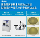
Plasma Debonding in Wafer Manufacturing
Shengding PLASMA glue removal technology
Shengding has insisted on deep cultivation of plasma surface cleaning and activation for many years. Around the semiconductor industry, Shengding has established a professional team to invest in research and development. So far, it has obtained a number of patents for plasma wafer deglue and etching. At the same time, Suzhou Semiconductor Equipment Co., Ltd. was established to continuously develop new applications in the wafer field.
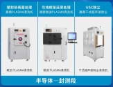
ICP plasma degumming machine
The ICP plasma degumming machine relies on Shengding's years of experience in photolithography and degumming, adopts a high-density, low-damage plasma source design, and is equipped with Shengding's mature remote ICP technology to achieve a high level of degumming rate and realize degumming Damage suppression; independent chamber structure design is adopted to achieve uniform flow field distribution and excellent adhesive removal uniformity.
RIE plasma degumming machine
RIE PLASMA remover is a cleaning equipment suitable for removing glue on the wafer surface of silicon-based materials. It can also be used for photoresist removal, silicon carbide etching, dry removal of hard mask layer, surface cleaning after etching, silicon oxide Or silicon nitride etching, DESCUM, photoresist removal between dielectrics and other applications, the scope of application of materials: 4-8 inches. The equipment is stable and reliable, easy to maintain and high in productivity.


纳安半导体 from suzhou is working on a GaN substrate project that will involve investment of 120m RMB & anticipate to produce 500m RMB when complete
I don't know much about these guys, but looks like a lot of substrate. btw, these are the things their Ga should be doing, moving up value chain, rather than just selling more raw ga
a few other GaN project listed there too for various power applications including Dongke semiconductor's project
I don't know much about these guys, but looks like a lot of substrate. btw, these are the things their Ga should be doing, moving up value chain, rather than just selling more raw ga
a few other GaN project listed there too for various power applications including Dongke semiconductor's project
No. No more comments needed for that.The questions are:
1. Can/do they really ban it?
Close to 100%.2. How much percentage can China be independent in legacy chip production? If China really relies on the West in legacy chip production and, one day, they ban it, China will be difficult even in EV production.
Nobody knows. Their so-call plans were completely nutz.3. Is EV the main target that they aim at?
Absolutely!Yellen said that the US only curb China chip at 14nm and lower, looks like her words sound like sh*t!
It is kind of like what Suz Tzu said, they lost before the fight even started, at least in the mature nodes.
more on 3rd gen semiconductor materials.
Hebei Sinopack says its is supplying BYD & Gree Electric with SiC MOSFET for testing & introduction
Demand for SiC is just exploding right now
They announced plans for expanding SiC capacity last year
worked out to be 120k wafers per year of 6-inch wafers
1.2 million GaN modules for 4G/5G base stations
as well as 24k SiC power modules (that doesn't seem like a lot)
and 12 million SiC SBD/MOSFET tubes
CETC affiliated companies like Hebei Sinopack has quite the capacity now
They signed up FAW last year
and now reported in October that they'd produce SiC MOSFET for BYD & Gree

See the organization chart here. Got all the 5G base station heavyweights as well as their own substrate producers and such
1200V is the main demand, but they are also producing 1700V and they are working on 3300V also.
Good to see this, since that means CETC cost will continue to come down which will lead to lower cost for their PLA related stuff also
Hebei Sinopack says its is supplying BYD & Gree Electric with SiC MOSFET for testing & introduction
Demand for SiC is just exploding right now
They announced plans for expanding SiC capacity last year
worked out to be 120k wafers per year of 6-inch wafers
1.2 million GaN modules for 4G/5G base stations
as well as 24k SiC power modules (that doesn't seem like a lot)
and 12 million SiC SBD/MOSFET tubes
CETC affiliated companies like Hebei Sinopack has quite the capacity now
They signed up FAW last year
and now reported in October that they'd produce SiC MOSFET for BYD & Gree

See the organization chart here. Got all the 5G base station heavyweights as well as their own substrate producers and such
1200V is the main demand, but they are also producing 1700V and they are working on 3300V also.
Good to see this, since that means CETC cost will continue to come down which will lead to lower cost for their PLA related stuff also
antiterror13
Brigadier
Bro its the other way around, how many FABS can produced chips at 7nm, only 2 TSMC and Samsung, next year you may include SMIC, all of them are Asian, that's the worry. Even if the US can harvest their 5nm tech the innovating center are still located in East Asia.
Now IF China flooded the market with 14nm and above chip how can the Collective West compete? only Intel if they successfully stole TSMC (which I doubt) 7nm and 5nm tech. Cost wise they price themselves out of the market if they insist on onshoring their production in the US.
Intel may have 7nm production facility this year or next year
The only thing Intel consistently produced in the last 5 years is delays.Intel may have 7nm production facility this year or next year
- Status
- Not open for further replies.


