Chinese semiconductor industry

Status
Not open for further replies.

tokenanalyst

Brigadier
Registered Member

Hangzhou Qiantang District signed a number of semiconductor projects, including Xingyuanchi Semiconductor, Bingbo Semiconductor, etc.​


According to news from Jiwei.com, recently, in the third quarter of 2023, the "Double Ten Billion" major investment promotion project signing ceremony and the intensive start-up of key industrial projects in Qiantang (New) District, Hangzhou City, Zhejiang Province were held. At the meeting, 8 major investment projects with a cumulative total investment of 11.1 billion yuan were signed, and 10 key industrial projects with a cumulative total investment of 10.6 billion yuan started construction.
225768063469.9081562365476650.0916.jpg


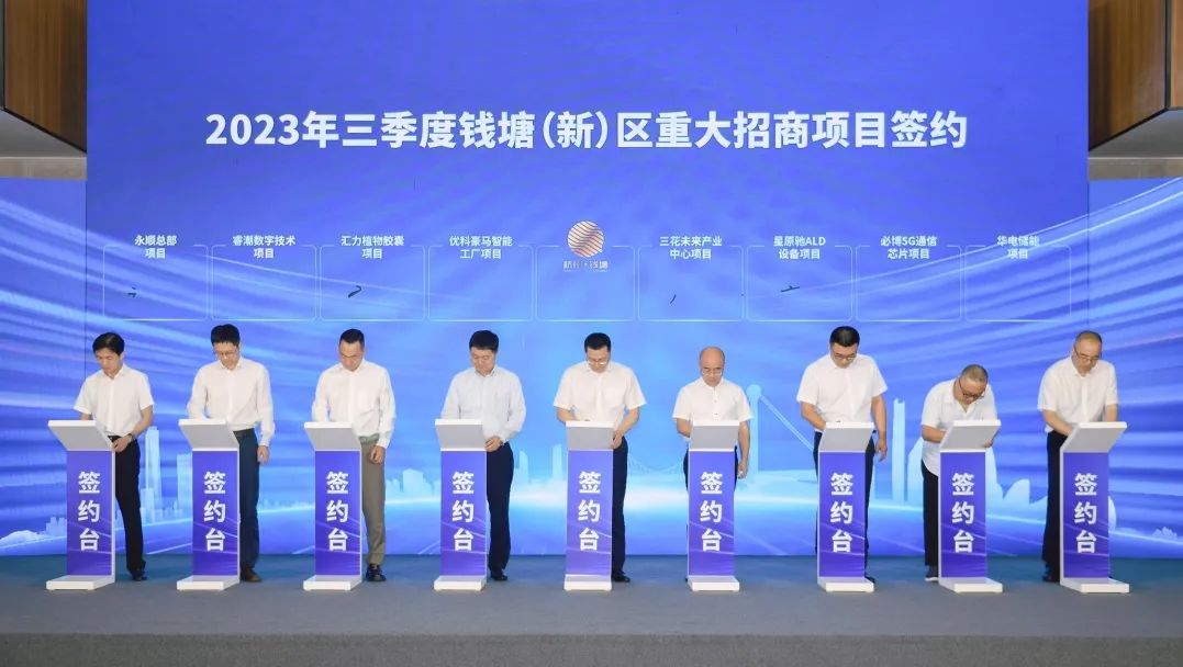
Some signed projects:
Xingyuanchi ALD atomic layer deposition equipment project

The investor of the project, Hangzhou Xingyuanchi Semiconductor Co., Ltd. is a design and manufacturer of ALD atomic layer deposition (vacuum precision coating) equipment for semiconductors, high-definition displays and advanced optics. The company's headquarters and future listing entities have settled in Qiantang. Its main product is ALD atomic layer deposition equipment. The project plans to invest a total of 1.6 billion yuan, including 448 million yuan in fixed assets and 726 million yuan in research and development.
Bibo Semiconductor Headquarters and 5G Communication Chip Project
Hangzhou Bibo Semiconductor Co., Ltd., the investor of the project, is committed to the research and development of key core chips and platform technologies for 5G communications such as the Internet of Things, Internet of Vehicles, and low-orbit satellites. The project starts from the simplified 5G (RedCap R17) IoT chip with high threshold. It is planned to complete the RF test chip engineering batch tape-out and FPGA field test in the second half of this year. The first batch of chips will be applied to smart grid, security, industrial control, etc. Application scenarios. The project has set up the company headquarters and future listed entities in Qiantang, with a planned total investment of 770 million yuan, and will carry out the research and development and design of 5G communication chips.
Zhejiang Ruichao Digital Technology Project
The investor of the project, Zhongruixin Digital Technology Co., Ltd., is a high-tech enterprise with heavy asset investment as its core business. The project is a digital economy industry project with a planned total investment of 450 million yuan, including 131 million yuan in research and development and 100 million yuan in fixed investment. The project will provide the government with a full range of IT nanny services and digital asset operation services through franchising, purchasing services and other modes, provide enterprises with a complete set of digital transformation solutions and operational application innovation, and provide residents with multi-scenario socialized operational services. Helping the transformation and upgrading of the digital government and the "smart digital transformation" of the industry.
Some start-up projects:
Qiantang Core Science and Technology Park Phase II Project

The project is located in Qiantang Xingu, east to Qingdong 2nd Road, south to Hangzhou Yibang Spandex Co., Ltd., Hangzhou Liangdahong Packaging Technology Co., Ltd., west to Hangzhou Tuobang Curtain Wall Technology Co., Ltd., Hangzhou Zhongyi Runyuan Industrial Co., Ltd. , north to Jiangdong Fifth Road. The total investment of the project is 1.608 billion yuan, the total land area is about 87,000 square meters, and the total construction area is about 247,400 square meters. It will build 9 high-rise factory buildings, 11 multi-storey factory buildings, 1 supporting building and an opening and closing office. The construction period of the project is 2023-2026, and the planned investment in 2023 is 50 million yuan.
KONE high-end transmission equipment intelligent manufacturing project
The project is located in Qianjin Intelligent Manufacturing Park, east to the planned greening of Qianjin Avenue, west to the planned greening of Dongwu River, and north to the planned greening of Dongwu River. The total investment of the project is 350 million yuan, the total land area is about 40,000 square meters, and the total construction area is about 124,000 square meters. It is planned to build 1 workshop and 1 comprehensive building, of which the comprehensive building includes R&D workshops and staff dormitories. The construction period of the project is 2023-2026, and the planned investment in 2023 is 80 million yuan.

Please, Log in or Register to view URLs content!
 

tokenanalyst

Brigadier
Registered Member

Gallium and Semiconductor received 65 million yuan in Series A financing​

Recently, Beijing Gallium and Semiconductor Co., Ltd. (hereinafter referred to as Gallium and Semiconductor) officially announced the completion of Series A financing of 65 million yuan, led by Kaishi Capital, Haitong Securities, Zhengwei Capital,
Recently, Beijing Gallium Semiconductor Co., Ltd. (hereinafter referred to as "Gallium Semiconductor") officially announced the completion of the A-round financing of 65 million yuan, led by Kaishi Capital, followed by Haitong Securities, Zhengwei Capital, and Yingtian Investment.
Chuangchenghui news shows that the team of Professor Tang, the founder of Gallium and Semiconductor, has been deeply involved in the field of gallium oxide for more than ten years, and has received support from more than ten scientific research funds such as the National Natural Science Foundation of China and the National Key Research and Development Program. Gallium and Semiconductor's current round of financing will further accelerate the development process in key links such as technological breakthroughs, product development, capacity expansion, talent introduction, and application layout, thereby contributing to the acceleration and upgrading of large-scale gallium oxide substrates and epitaxial localization.
Gallium and Semiconductor was established in 2021. It is a gallium oxide substrate and epitaxial manufacturer of ultra-wide bandgap semiconductor materials. It is mainly engaged in gallium oxide single crystal substrates and epitaxial wafers, single crystal and epitaxial growth equipment, and high-sensitivity solar-blind ultraviolet detection. Gallium oxide-related products such as devices and high-power power electronic devices.
Since its establishment, Gallium Semiconductor has applied for 18 domestic invention patents, and has four core technologies: gallium oxide single crystal growth technology, gallium oxide substrate processing technology, gallium oxide thin film epitaxy technology, and gallium oxide device technology.

Please, Log in or Register to view URLs content!
 

tokenanalyst

Brigadier
Registered Member
Low-energy large-beam ion implanter iStellar-500 series products

1690819263927.png
Purpose: iStellar-500 series products are a series of low-energy and large-beam ion implanters launched by Kaishitong. The products adopt the "general platform + key technology module" research and development model, quickly iteratively upgrade and broaden the product line of ion implanters, covering different chip pairs The needs of ion implantation are positioned to provide customers with products with higher reliability and lower cost of ownership, and have good production line process matching capabilities and extensive process coverage capabilities.


Features: high-precision injection angle control, particle pollution control, realization of -100° ultra-low temperature injection, mass production of mainstream FAB production lines


High energy ion implanter iStellar-HE2000

1690819331654.png

Purpose: iStellar-HE2000 is a high-energy and large-beam ion implanter product launched by Kaishitong. It adopts the "general platform + key technology module" research and development model, and key technologies such as high-pressure acceleration, high injection angle accuracy, and nano-scale particle pollution control meet the requirements of High-energy ion implantation requirements for chip manufacturing. istellar-HE2000 products are continuously improved through technical modules to provide customers with products with higher reliability and lower cost of ownership.


Features: high-precision injection angle control, particle pollution control, metal pollution control, localization of parts and independent supply
 

tokenanalyst

Brigadier
Registered Member
Using the chip "Jia" to support: Jiaxin Semiconductor's one-stop solution shows its hard power

Jiaxin Semiconductor Equipment Technology Co., Ltd. was established in 2021 by Wanye and world-renowned semiconductor industry experts. At this stage, it has formed three core sectors: Jiaxin Caneng Subsidiary, Jiaxin Hongyang Subsidiary and New Product R&D Department. Jiaxin Semiconductor will successively lay out the R&D and manufacturing of 8-inch/12-inch semiconductor front-end equipment to provide high-performance products for the current mainstream mature processes. At present, the company has successively introduced to the market a variety of semiconductor equipment covering etching machines, thin film deposition, rapid heat treatment, etc., which can provide customers with one-stop solutions.

One-stop solution for integrated circuit front-end equipment

Jiaxin Semiconductor integrated circuit front-end equipment one-stop solution
1690819423289.png


Starting from the whole process, Jiaxin Semiconductor covers the main process equipment such as CVD/PVD/etching → vacuum pump → exhaust gas treatment equipment, and builds a one-stop equipment solution for customers.

Since the second half of 2022, Jiaxin Semiconductor has won multiple bids for a variety of equipment, including silicon nitride plasma etching machines, metal plasma etching machines, sidewall plasma etching machines, high-density plasma thin film deposition equipment (HDP-CVD), Silicon dioxide plasma thin film deposition equipment (PECVD), boron phosphorus doped silicon dioxide thin film chemical deposition equipment (SACVD), titanium/titanium nitride deposition equipment (MOCVD), aluminum copper metal sputtering equipment (PVD) and rapid heat treatment ( RTP), etc.

1690819489988.png


On the first day of the exhibition, the integrated circuit front-end equipment products of Kaishitong and Jiaxin Semiconductor, a subsidiary of Wanye Enterprise, received high attention and affirmation from the participants. The company also discussed project cooperation and cooperation models with customers in the semiconductor industry chain. In-depth discussions and exchanges.

In the future, Wanye Enterprise will also insist on implementing the "1+N" equipment platform model, based on Kaishitong ion implanter, taking Jiaxin Semiconductor as the industry extension tentacles, and laying out the core equipment of integrated circuits in multiple directions to serve more Customers provide one-stop solutions to contribute to the localization of integrated circuit equipment manufacturing!

Please, Log in or Register to view URLs content!
 

tokenanalyst

Brigadier
Registered Member

Jingsheng Electromechanical: has mastered the industry-leading 8-inch silicon carbide substrate process and technology​

Recently, Jingsheng Electromechanical stated on the interactive platform that the company has mastered the industry-leading 8-inch silicon carbide substrate process and technology. The company has successfully grown an 8-inch silicon carbide substrate through multiple rounds of diameter expansion through its own seed
Recently, Jingsheng Electromechanical stated on the interactive platform that the company has mastered the industry-leading 8-inch silicon carbide substrate process and technology. The company has successfully grown an 8-inch N-type silicon carbide crystal through multiple rounds of diameter expansion through its own seed crystal, solving the problem of Difficult problems such as uneven temperature field, crystal cracking, and distribution of gas phase raw materials during the growth of 8-inch silicon carbide crystals were solved. The company has built a research and development experimental line for 6-8 inch silicon carbide crystal growth, slicing and polishing, and accelerated the development process of silicon carbide substrate materials by continuously strengthening technological innovation and process accumulation.

1690820710449.png

Please, Log in or Register to view URLs content!
 

tokenanalyst

Brigadier
Registered Member

The second phase of Jita Semiconductor's characteristic process production line welcomes new progress!​


According to the China Construction Eighth Bureau Development and Construction Company, the total construction area of the project is 220,000 square meters, and the construction period is about 600 days. After the project is completed, it will further improve the domestic chip manufacturing technology level, truly break the bottleneck of domestic automotive chip manufacturing technology, and solve the "stuck neck" problem.

As a "under construction" project, Jita Semiconductor's characteristic process production line project has been continuously listed on the list of major construction projects in Shanghai in 2022 and the list of major projects in Shanghai in 2023.

According to previous reports, Jita Semiconductor's characteristic process production line construction project is located in the I02-02 plot of Lingang Heavy Equipment Industrial Zone, Pudong New Area, Shanghai. The project is divided into two phases. The first phase will be completed in 2020, and the second phase is the Jita Semiconductor advanced car-grade chip expansion project that started construction (August 22, 2022). The total construction area of the project is 220,000 square meters, and the construction period is about 600 days. After the completion of the second phase of the project, the production capacity of Jita Semiconductor will be greatly improved, and the scale level of the factory in the free trade zone will be further improved, and the mass production of automotive chips such as power devices, analog ICs, and MCU products will be realized. The production capacity of 300,000 8-inch equivalent wafers.
On June 2 this year, Jita Semiconductor's 12-inch automotive chip lead wire was completed . The 12-inch BCD products of this production line were officially launched in February this year, and the tape-out was completed on June 2, and the electrical (WAT) test results of the components all met the standards.

Please, Log in or Register to view URLs content!
 

KYli

Brigadier
Importing less foreign chips and equipment can be said that China's tech ambition has been hindered by the sanctions. On the other hand, it could also be a sign of self reliance and cut back of needing Western components and inputs. At the same time, the recent downturn of SMIC sector has both lowered the chips prices and demands.
Please, Log in or Register to view URLs content!

Please, Log in or Register to view URLs content!
 

sunnymaxi

Captain
Registered Member
Importing less foreign chips and equipment can be said that China's tech ambition has been hindered by the sanctions. On the other hand, it could also be a sign of self reliance and cut back of needing Western components and inputs. At the same time, the recent downturn of SMIC sector has both lowered the chips prices and demands.
Please, Log in or Register to view URLs content!

Please, Log in or Register to view URLs content!
another useless article bro .. so much copium

5rXIJ0Ag.jpg

NAURA/AMEC and other Chinese tools makers have record earning in 2022. from 50% to 100% YOY jump in revenue.

28nm supply chain has completed. West/Japan can only cry now.
 
Last edited:

AndrewS

Brigadier
Registered Member
From today's Baiguan substack newsletter (not me)

---

The Chip War might just be what China needs right now
“The Chip War cannot be rushed, but the War of AI cannot be delayed”

ROBERT WU
JUL 31

Today, we are presenting an interesting article on China-US tech rivalry, because in our eyes it reflects how many of the Chinese elite look at the US technology ban on China. These are the main ideas of the article:

  • One important consequence of the US embargo is that it helps create a huge market demand for China’s semiconductor industry, so the market mechanism replaces government subsidies as the main driving force.
  • Building a domestic semiconductor industry is hard, and will take very long time, but China is no stranger to this type of development. It’s only a matter of when and how fast.
  • However, the revolution in artificial intelligence adds a new variable to the game, something China must seize on as quickly as possible (you may read here on how Chinese government is responding with the final version of AIGC regulation).
  • The original article is written by Boss Dai 戴老板, a famous technology and business influencer in China. Our translation is not reviewed by the author.
---


关于芯片战争的二三事 A few things about the Chip War

mp.weixin.qq.com/s/BNl8fnzB_hgXs6Wd7OExgg?utm_source=substack&utm_medium=email

By Boss Dai

Recently, Janet Yellen visited China with reportedly many "tasks" to accomplish. Foreign media summarized one of her tasks as "convincing Chinese officials that the series of measures taken by the US to prevent China from accessing sensitive technologies such as semiconductors in the name of national security is not intended to harm the Chinese economy."

It is already 2023, and the US has launched more than ten rounds of bans on China's chip industry. The number of mainland enterprises and individuals on the entity list has exceeded 2,000. It is heartwarming that they can still come up with such a noble reason.

It is estimated that even the Americans cannot stand it anymore. This statement was soon refuted by another article on the New York Times.

Four days after Yellen left China, Alex Palmer, a well-known China reporter for foreign media, published an article in the NYT that explained the essence of the US chip blockade in the title: "This is an Act of War."

Alex Palmer graduated from Harvard and was among the first Yenching Scholar at Peking University. He has been reporting on China for a long time, covering topics such as Xu Xiang, fentanyl, and TikTok. He is a familiar figure who has been “hurting the feelings of the Chinese people”. However, in the matter of chip technology, he managed to extract the truth from the Americans.

In the article, one interviewee bluntly stated, "Not only will we not allow China to make any technological progress, but we will also actively reverse their current technological level." The chip ban is essentially aimed at eradicating China's entire advanced technology ecosystem.

The Americans used the word "eradicate," which carries the meanings of "exterminate" and "uproot," often associated with diseases like smallpox or Mexican drug cartels. Now, this word is being used to describe China's high-tech industry. The author predicts in the article that if these measures succeed, it could impact the progress of an entire generation in China.

Anyone who wants to understand the severity of this war only needs to repeatedly ponder the word "eradicate."

An upgraded war

The rules of competition and the rules of war are two completely different things. Business competition is a contest under legal framework, but war is different. The opponent will almost never consider any rules or restrictions and will do whatever it takes to achieve their strategic objectives. Especially in the chip industry, the United States can even keep changing the rules - as soon as you adapt to one set, it will immediately switch to a new one to deal with you.

For example, in 2018, the US Department of Commerce sanctioned Fujian Jinhua by using the "Entity List," directly leading to the latter's shutdown (which has since resumed operations); after this kind of small success, [The US Government] also included Huawei in the Entity List in 2019, restricting US companies from providing products and services to it, such as EDA software and Google's GMS.

After discovering that these methods were not enough to completely "eradicate" Huawei, the US changed the rules: starting in May 2020, all companies using US technology could not supply Huawei, such as TSMC's foundry. This directly led to the stagnation of HiSilicon and the significant decline of Huawei's smartphones, bringing more than 100 billion yuan in losses to the Chinese industrial chain every year.

Afterward, the Biden administration escalated its targets from "companies" to "industries," and a large number of Chinese companies, universities, and research institutions were subsequently included in the ban list. On October 7, 2022, the Bureau of Industry and Security (BIS) of the U.S. Department of Commerce issued new export control regulations, effectively imposing a "ceiling" on Chinese semiconductors. Logic chips below 16nm or 14nm, NAND storage with 128 layers or more, and integrated circuits (DRAM) below 18nm are restricted from export. Additionally, computing chips with a performance exceeding 4800 TOPS and interconnection bandwidth exceeding 600GB/s are also restricted from supply, whether through manufacturing or direct sales.

Using the words of a Washington think tank: Trump targeted companies, while Biden is targeting industries.

When reading the novel "The Three-Body Problem," ordinary readers can easily understand the plot of the Trisolarans to lock down Earth's technology [Baiguan note: This novel is a widely-read and widely-cited Chinese sci-fi series, in which the aliens, called the Trisolorans, used a super technology to keep a lid on basic science research on Earth]. However, in real life, many non-industry individuals tend to have a certain perception when observing the chip ban: as long as you comply with U.S. rules, you won't be targeted; if you are targeted, it means you did something wrong.

Having such a perception is normal because many people's thinking is still within the framework of "competition." However, in a “war”, this perception may be just an illusion. In recent years, many semiconductor executives have expressed that when a company ventures into advanced fields in R&D (even just in preliminary research), they will encounter an invisible barrier.

The development of high-end chips is based on a global technology supply chain. For example, to make a 5nm SoC chip, one needs to license from ARM, software from Cadence or Synopsys, patents from Qualcomm, and coordinate production capacity with TSMC. By doing these actions, one will come under the purview of the BIS’s regulations.

A case in point is a chip company under a certain smartphone manufacturer, which set up a R&D subsidiary in Taiwan to attract local talent for consumer-grade chips. However, it soon encountered an "investigation" by relevant Taiwanese authorities. Helpless, this subsidiary was separated from its parent company and became an independent supplier, but still had to proceed with caution.

In the end, after a raid and seizure of servers by Taiwanese "inspecting authorities" (where no violations were found), this Taiwanese subsidiary was forced to shut down. A few months later, its parent company voluntarily dissolved as well - senior management realized that under constantly changing restrictions, any high-end chip project carried the risk of being "reset with a single button”.

[redacted]

This ability to "reset with a single button" essentially turns the previously practiced "global division of labor based on free trade" into a weapon for attacking enemies. To whitewash this behavior, American scholars have even coined a term: weaponized interdependence.

Once these facts are clear, many previously disputed matters no longer need to be discussed. For example, it is pointless to mock Huawei for violating the Iran sanctions because they have already stated clearly that "Iran is just an excuse." Likewise, criticizing China's industrial policies seems ridiculous, as the US promptly allocated $53 billion to subsidize chip manufacturing and promote re-shoring.

As Carl von Clausewitz once said, "War is the continuation of politics." The same can be said for the Chip War.

Cont...
 
Last edited:

AndrewS

Brigadier
Registered Member
...cont

the blockade can backfire

Some may ask: Is there really no way to respond to the US's "all-out war"?

If you're looking for a miraculous move that can defeat the enemy in one stroke, there really isn't one. Computer technology itself, including the integrated circuit industry, was born in the US. By using war tactics to exert dominance over the industrial chain, China can only take longer to conquer the upstream and downstream bit by bit. This is a long process.

However, if one is to think this "war behavior" doesn't have any side effects and can be used continuously, it is not true. The biggest side effect of this all-industry blockade by the United States is that it has given China the opportunity to rely on market mechanisms – rather than pure planning power – to solve the problem of “卡脖子 technology stranglehold”.

This sentence may seem difficult to understand at first. We can first understand what “pure planning power” means. For example, in the semiconductor industry, there is a project that specifically supports major technological breakthroughs called the "Manufacturing Technology and Complete Set of Processes for Ultra-Large-Scale Integrated Circuits," commonly known as the “02 Special Project”, which is funded purely by government finances.

Many companies have received funding from the 02 Special Project. When I was researching semiconductor companies, I saw many prototypes left over from this project. After seeing them, I had mixed feelings. Although the 02 Special Project provided valuable funding for companies during the economic downturn, the efficiency of using these funds was not high. Even if the funds were given to the companies in the form of subsidies, it was difficult to produce technologies and products that could enter the market. People who have done scientific research probably understand this.

Before the chip war, China had many struggling equipment, material, and small chip companies that were difficult to compete with foreign counterparts. Companies like SMIC, JCET, and even Huawei did not pay much attention to them because they could buy more mature and cost-effective foreign products. However, the US blockade of the Chinese chip industry has brought a rare opportunity for these companies.

Under the blockade, domestic companies that were previously ignored by wafer fabs or test and packaging factories were pushed to the forefront. A large number of equipment and materials were sent to production lines for validation. Domestic small factories suddenly saw hope, and no one dared to waste this precious opportunity. Therefore, they burnt the midnight oil to improve their products.

Although this is a forced market mechanism, an internal circulation market mechanism, its efficiency is much higher than pure planning: one party is determined to replace imports, while the other is desperately holding onto a lifeline. Under the inspirations of wealth creation effects of the Shanghai STAR Board, almost every vertical segment of the semiconductor upstream has many companies involved.

I asked my colleagues to compile the profit trends of Chinese semiconductor listed companies over the past decade (only selecting companies with ten years of continuous performance). There is an obvious growth trend: ten years ago, the total profits of these domestic companies was only more than 3 billion, and by 2022, their total profits exceeded 33.4 billion, nearly ten times that of ten years ago.


Alex Palmer commented in his article: When Chinese companies can access Western chip suppliers, domestic manufacturers do not have much business. But now, if Chinese companies do not unite, the outcome will be collective destruction. "Previously, they could choose between national resilience and business development, but now this choice no longer exists."

Of course, some people may question: "These domestic alternatives are all in the mid-to-low-end field. We still cannot break through in the high-end chip market." This questioning is not unfounded from a factual perspective. However, chips are not like the internet, where a few programmers can come up with something in a few months. It is an industry that requires years of investment and development, and it cannot be rushed.

In the past decade, the domestic semiconductor industry has made significant progress. However, public opinion often has a tendency to focus on lithography, to the extent that the belief "if China cannot produce EUV lithography machines, its semiconductor industry is not capable" has become very popular. This viewpoint is neither objective nor correct, and it obscures the efforts and hard work of many people, but it is widely embraced.

Of course, the success of an industry ultimately depends on whether it possesses the necessary conditions for success, such as funding, talent, and market. This is not greatly influenced by public opinion. Moreover, many extremely pessimistic remarks have appeared not only recently, but also many years ago in fields such as high-speed rail, wind power, solar power, and new energy vehicles.

Cont...
 
Status
Not open for further replies.
Top