Chinese semiconductor industry

Status
Not open for further replies.

tokenanalyst

Brigadier
Registered Member

Zhejiang Unicmicro's 6-inch silicon-based wafer foundry project is expected to increase the volume of Q4 products​


Recently, Zhejiang Unic Microelectronics' 6-inch high-end characteristic silicon-based wafer foundry project has made new progress.
According to the news from Lishui Economic and Technological Development Zone, at present, the main construction of the Unicmicro project has been basically completed, the civil engineering has entered the final acceptance stage, the factory service system has been completed, and the installation and debugging of Fab1-A’s entry equipment has been completed. It is expected that the production volume will increase in the fourth quarter of this year.
Zhejiang Guangxin Microelectronics project will be carried out in two phases, with a planned total investment of 2.4 billion yuan and a land area of 148 mu. It will mainly build a 6-inch silicon-based wafer production line . After completion, it will be able to form an annual production capacity equivalent to 2.4 million 6-inch silicon-based power semiconductor wafers and 36,000 third-generation semiconductor silicon carbide and gallium nitride wafers.
It is understood that Zhejiang Guangxin Microelectronics Co., Ltd. was established in 2021, focusing on automotive electronics, energy revolution, industrial control and other application fields. In the key construction project plan of Zhejiang Province in 2023, Zhejiang Unicmicro's 6-inch high-end characteristic silicon-based wafer foundry project is listed.

Please, Log in or Register to view URLs content!
 

tokenanalyst

Brigadier
Registered Member

Sanan established a semiconductor company in Chongqing with a registered capital of 1.8 billion yuan​


Tianyan Check shows that Chongqing Sanan Semiconductor Co., Ltd. was incorporated on July 8. The legal representative is Cai Wenbi, with a registered capital of 1.8 billion yuan .

Shareholder information shows that Hunan Sanan Semiconductor Co., Ltd. holds 100% of Chongqing Sanan Semiconductor Co., Ltd.

On June 8, Sanan Optoelectronics Co., Ltd. (hereinafter referred to as " Sanan Optoelectronics ") and STMicroelectronics signed a cooperation agreement on the Chongqing Sanan STMicroelectronics silicon carbide project. According to the agreement, STMicroelectronics and Sanan Optoelectronics will establish a joint venture company to promote the construction of Sanan STMicroelectronics silicon carbide project.

On June 9 , "STMicroelectronics China" reported that the two parties will establish a new 8-inch silicon carbide device joint venture manufacturing plant in Chongqing. The new SiC fab is scheduled to start production in the fourth quarter of 2025 and is expected to be fully inaugurated in 2028, when it will better support China's growing demand for automotive electrification, industrial power and energy applications. At the same time, Sanan Optoelectronics will use its own SiC substrate process to independently build and operate a new 8-inch SiC substrate manufacturing plant to meet the substrate needs of the joint venture plant.

Please, Log in or Register to view URLs content!
 

WTAN

Junior Member
Registered Member
Sir ASML try to restrict sales of NXT 2000i to China, well good luck with that, like I said before anything below NXT 2000i is a non starter, now with this rumor only NXT 2050i can do. :)

And the window is closing very fast for ASML as @olalavn once mentioned the year 2024 is the inflection point, I believed him fully as the momentum is gaining strength to strength as posted here by Prof @tokenanalyst.
Yes, looks like SMEE is quickly catching up to ASML.
Chinese FABS will have to rely on the SMEE 28NM DUVL as its primary Lithograph for mass production due to the product restrictions by ASML and Nikon.
 

tokenanalyst

Brigadier
Registered Member

University of Electronic Science and Technology of China Luo Xiaorong's research group has made research progress in the field of ultra-wide bandgap semiconductor gallium oxide power devices.​


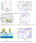
Due to its ultra-wide bandgap and high critical breakdown electric field, gallium oxide, a semiconductor material, has a Barrega figure of merit (3444) that is much greater than that of SiC (340) and GaN (870), and can grow high-quality, large-size single crystals through a variety of lower-cost melt methods, which can meet the development needs of high-power, high-efficiency, and miniaturization of new-generation power systems and power electronic devices. Gallium oxide is clearly listed as an export control by a certain country. Recently, my country has also implemented export controls on gallium and germanium-related items. Gallium oxide has become a must-see for international science and technology strategy, and is a hot spot and focus of research at home and abroad. In recent years, the research group of Professor Luo Xiaorong from the University of Electronic Science and Technology of China has started the research on ultra-wide bandgap gallium oxide devices, and has made a series of new progress in the research of new gallium oxide power rectifiers and transistors and their reliability.

1690293389738.png

Please, Log in or Register to view URLs content!
 

tokenanalyst

Brigadier
Registered Member

Big news from Huawei! The latest achievements in the semiconductor field are unveiled: EDA has made an important breakthrough!​


At the 2023 World Semiconductor Conference and Nanjing International Semiconductor Expo held last week, Huawei exhibited EDA solutions based on computing and storage capabilities. It covers semiconductor electronics solutions in R&D, production, supply and operation, including specific applications such as full wireless factories, FAB micro-isolation, AI quality inspection, yield big data, and EDA engineering simulation.

It is understood that the EDA solution displayed by Huawei is mainly based on its internal computing, storage and network platforms, and adapts to the needs of different scenarios with end-to-end full service capabilities.

In terms of AI tool-assisted improvement of production quality inspection, Huawei has joined forces with industrial partners such as Bohan Intelligence, Chuangda, and Jushi Technology to jointly create AI quality inspection solutions for electronics, new energy, and semiconductors.

At the same time, Huawei also provides a joint solution of the YMS yield management system based on its big data platform base, which supports a maximum of 10P-level data processing capabilities.

For our country, the localization of EDA chip design software is of great significance to the breakthrough in the chip field, and its significance is as important as the localization of lithography machine manufacturing.

Please, Log in or Register to view URLs content!
 

tokenanalyst

Brigadier
Registered Member

The first domestic 12-inch Online epitaxial film thickness measurement equipment​


Recently, GEZE Semiconductor announced that the 12-inch measurement equipment GS-A12X independently developed by the company will be delivered soon. This equipment is the first 12-inch Online epitaxial film thickness measurement equipment in China, which can accurately measure the epitaxial film thickness of various wafer materials, and can ensure the accuracy and safety of the measurement.

Wafer preparation includes substrate preparation and epitaxy process. Epitaxy refers to the process of growing a new single crystal on a single crystal substrate. The epitaxy process may be affected by various conditions and factors such as substrate temperature, reaction chamber pressure, reaction growth, and wafer surface cleaning process. If the epitaxial thickness is not uniform in the active area of the transistor device fabricated on the wafer surface, it will lead to device failure. Therefore, after the wafer is prepared by the epitaxy process, it is particularly important to measure the thickness uniformity of the epitaxy using a film thickness measurement device.

1690294546363.png

The GS-A12X uses a dual-arm cleaning manipulator with a walking axis, and the measurement unit uses a newly designed Stage platform, which can choose adsorption or clamping methods, and is more compatible with customer application scenarios. The cooperation of the dual-arm manipulator and the Stage makes the measurement efficiency of GS-A12X increase by at least 30%. The design and application of the air-floating platform reduces the impact of vibration on measurement and makes the measurement data more stable. -A12X understands customers better.


Based on FTIR infrared spectroscopy technology, the equipment can monitor real-time data during the wafer epitaxy manufacturing process online and provide high-precision test results. Its main features include the following:

  • Efficient and fast: Using fast scanning technology, it can obtain high-precision test data in a short time and improve production efficiency;
  • Non-intrusive detection: using infrared spectroscopy technology, it will not cause any damage or impact on the wafer, ensuring that the test data is true and reliable;
  • High reliability: high-quality materials and advanced technology are used to ensure the stability and reliability of the equipment;
  • Data analysis: The equipment comes with data analysis software, which can realize data visualization and help users better understand the performance and characteristics of wafers;
  • Customized function development: Customized development for the pain points of customer applications, so that the system can better understand customers.
Online technology

The equipment delivered this time has added Online online technology. The device follows the SEMI standard protocol and can be seamlessly connected to customer OHT/MES and other systems. At the same time, the equipment realizes automatic detection control, has intelligent control and automatic operation functions, reduces labor costs and improves production efficiency.

Large size wafer inspection technology

Compared with 6-inch and 8-inch wafer measurement equipment, 12-inch wafer measurement equipment requires higher technical support in automation, communication, algorithms and other aspects. The newly launched GS-A12X equipment breaks professional barriers and uses more advanced detection technology to meet the inspection needs of fabs for 12-inch large-size wafers and help fabs reduce costs and increase efficiency.

Please, Log in or Register to view URLs content!
 

tphuang

Lieutenant General
Staff member
Super Moderator
VIP Professional
Registered Member
Is a non official source but let's see what happens.
The implication is big
Screen Shot 2023-07-25 at 10.10.52 AM.png
Depending on how much you want to believe this poster. They have a new kirin chip with daily production of 32k, which works out to a million a month. If we assume about 300 chips per wafer, then that's 3000 wafers a month, which is 35 to 40% of SMIC's current 7nm capacity. So just bringing back kirin chip for 1 medium ranged phone pretty much taps out all of SMIC's current 7nm capacity (since they are still producing HPC chips for various vendors) and this is not even factoring the 5G chipsets that they also need

Something with 2000i type of overlay precision theoretically allows them to have all domestic 7nm production line, although I would imagine they try it with 14nm first. Either way, it would allow them to drastically expand 7nm production by 2025.
 

ZeEa5KPul

Colonel
Registered Member
Yes, looks like SMEE is quickly catching up to ASML.
Chinese FABS will have to rely on the SMEE 28NM DUVL as its primary Lithograph for mass production due to the product restrictions by ASML and Nikon.
I had a couple of questions. Are you hearing this news about SMEE benchmarking against 2000i from your own sources? Can we conclude from this that benchmarking against 1980Di has been successful and SMEE can now match those parameters?
 

tokenanalyst

Brigadier
Registered Member
193nm is the wavelength of the DUVL light source.

Lithography machines using such a light source can handle at least the 7 nm process node or even 5 nm. (Assuming all the other process-node technical challenges are solved)
Is way more than the light source.
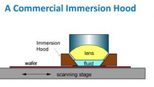
-There is a need for enhance resolution techniques like immersion liquids
1690297797699.png
- Also especial diffractive-refractive optics lens systems.
1690297743802.png
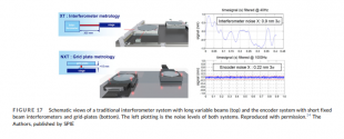
-Advance nanopositioning systems
1690297992620.png
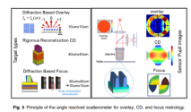
-Overlay and optics metrology
1690298163402.png

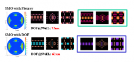
-Computational lithography
1690298303928.png

-And the photoresist and coating process.

When you add all that to techniques like a multi-patterning process then you can call something that is definitely no 7nm a 7nm process.
 
Status
Not open for further replies.
Top