Chinese semiconductor industry

Status
Not open for further replies.

tphuang

Lieutenant General
Staff member
Super Moderator
VIP Professional
Registered Member
Please, Log in or Register to view URLs content!
Moore Threads is one of the founding 24 members of China Mobile's metaverse industry alliance. The virtual world likely to require a lot of computational power for graphics rendering, simulation, AIGC and such. Looks like Huawei & MT are the main hardware suppliers of this. Although, I wouldn't be surprised if China Mobile is also using a lot of Nvidia GPUs

This to me seems like an area where American tech companies just haven't been interested in. I wonder if demand for this is higher in Asia or why the interest is so much greater for this among Chinese tech companies
Please, Log in or Register to view URLs content!
China Mobile looking to increase computation power from 8 to 20 EFLOPS by 2025


Also, I was looking up other Chinese AI companies to see how much domestic GPUs they use.

Please, Log in or Register to view URLs content!
From here last year, Sensetime's Lingang data center was using 5 domestic GPUs for 15% of its computational power there. A lof of things have changed in the past year. But one would imagine if Nvidia GPUs are banned, there is a pretty large market for domestic chipmakers to expand into
上海临港新一代人工智能计算中心AIDC于2022年1月24日正式启用,基于技术突破及芯片性能提升,临港AIDC峰值算力预计将比原设计峰值扩大33%达5 exaFLOPS;已上线算力达1.745exaFLOPS;已实现5种国产芯片适配,国产化算力规模占已上线规模的15%。
 

tokenanalyst

Brigadier
Registered Member

Topband Hongji received tens of millions of investment, focusing on 8/12-inch semiconductor quartz consumables, etc.​


Recently, Fosun Chuangfu completed an industrial investment of tens of millions of yuan in Liaoning Topband Hongji Semiconductor Materials Co., Ltd. (hereinafter referred to as "Topband Hongji"), supporting it to improve the localization of key quartz consumables in the fields of semiconductors and photovoltaics.
According to information from Fosun Chuangfu, Topband Hongji was established in May 2017. Its main business is the research and development, production and sales of 8-inch and 12-inch semiconductor quartz products and photovoltaic quartz products. The products are widely used in the production of semiconductor chips and solar energy. In the fields of photovoltaic, optical fiber, LED, electric light source, etc., the core team has a profound industrial background, with an average of more than 15 years of experience in the semiconductor quartz product industry. Since its establishment, Topband Hongji has developed a new production process based on the traditional production process, under the guidance of the semiconductor localization policy, combined with modern intelligent manufacturing technology, and realized an intelligent and automated production mode.​
 

SanWenYu

Captain
Registered Member
CETC's ion implanters now cover the "full process" in 28nm node.

Please, Log in or Register to view URLs content!

中国电科实现国产离子注入机28纳米工艺全覆盖​

新华社记者6月29日从中国电子科技集团有限公司获悉,该集团旗下中电科电子装备集团有限公司(简称电科装备)已实现国产离子注入机28纳米工艺制程全覆盖,有力保障我国集成电路制造行业在成熟制程领域的产业安全。

离子注入机是芯片制造中的关键装备。在芯片制造过程中,需要掺入不同种类的元素按预定方式改变材料的电性能,这些元素以带电离子的形式被加速至预定能量并注入至特定半导体材料中,离子注入机就是执行这一掺杂工艺的芯片制造设备。

当前,28纳米是芯片应用领域中覆盖面最广的成熟制程。据介绍,电科装备连续突破光路、控制、软件等关键模块的核心技术,形成中束流、大束流、高能及第三代半导体等全系列离子注入机产品格局,实现了28纳米工艺制程全覆盖,切实保障国产芯片生产制造。

据了解,作为国内最早从事离子注入设备研制及产业化的企业,电科装备已具备从产品设计到量产应用的完整研制体系,产品涵盖逻辑器件、存储器件、功率器件、传感器等工艺器件,百台设备广泛应用于国内各大集成电路先进产线,累计流片2000万片,有力提升我国产业链供应链韧性和安全水平。(记者温竞华)
 
D

Deleted member 24525

Guest
CETC's ion implanters now cover the "full process" in 28nm node.

Please, Log in or Register to view URLs content!

CETC achieves full coverage of 28nm technology for domestic ion implanters​

A reporter from Xinhua News Agency learned from China Electronics Technology Group Co., Ltd. on June 29 that the group's China Electronics Technology Electronic Equipment Group Co., Ltd. (referred to as Electronic Technology Equipment) has achieved full coverage of the 28-nanometer process of domestic ion implanters, which effectively guarantees my country's integration. Industrial safety of the circuit manufacturing industry in the mature process field.

Ion implanters are key equipment in chip manufacturing. In the chip manufacturing process, it is necessary to dope different kinds of elements to change the electrical properties of the material in a predetermined way. These elements are accelerated to a predetermined energy in the form of charged ions and implanted into a specific semiconductor material. The ion implanter performs this doping. Miscellaneous chip manufacturing equipment.

At present, 28nm is the mature process with the widest coverage in the chip application field. According to reports, Dianke Equipment has continuously made breakthroughs in the core technologies of key modules such as optical path, control, and software, and has formed a product structure of a full range of ion implanters including medium beam current, large beam current, high energy, and third-generation semiconductors. Coverage, effectively guarantee the production and manufacture of domestic chips.

It is understood that as the earliest enterprise engaged in the development and industrialization of ion implantation equipment in China, Dianke Equipment has a complete development system from product design to mass production application, and its products cover logic devices, storage devices, power devices, sensors and other process devices. Hundreds of equipment are widely used in the advanced production lines of major integrated circuits in China, with a cumulative tape-out of 20 million pieces, which has effectively improved the resilience and security level of my country's industrial chain supply chain. (Reporter Wen Jinghua)
What does full coverage mean in the context of ion implanters?
 

SanWenYu

Captain
Registered Member
What does full coverage mean in the context of ion implanters?
No idea. My uneducated guess is that ion implanters are used in different steps in the process and each has different requirements. Now the domestic implanters can meet all the requirements for 28nm. But I am not in this field.

Waiting for our in house experts to explain.
 

tokenanalyst

Brigadier
Registered Member
What does full coverage mean in the context of ion implanters?
Ion implanters are classified by their current and their energy. So I think they mean that they can manage the doping using an array of elements in the 28nm process, some elements require high energy while others the doping has to be more docile.

Apart that they have ion implanters for photovoltaic and third gen semiconductors.
 

tokenanalyst

Brigadier
Registered Member
No idea. My uneducated guess is that ion implanters are used in different steps in the process and each has different requirements. Now the domestic implanters can meet all the requirements for 28nm. But I am not in this field.

Waiting for our in house experts to explain.

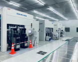
Another breakthrough! Dianke Equipment has achieved full coverage of ion implantation equipment in the 28nm process​


1688075166039.png
It is reported that the ion implanter is the key equipment in chip manufacturing, and 28nm is the mature process with the widest coverage in the current chip application field. Dianke Equipment has continuously made breakthroughs in the core technologies of key modules such as optical path, control, and software, and has formed a product structure of a full range of ion implanters such as medium beam current, large beam current, high energy, and third-generation semiconductors, and achieved full coverage of the 28-nanometer process. Guarantee the production and manufacturing of China's "chip".

Please, Log in or Register to view URLs content!
 

tokenanalyst

Brigadier
Registered Member

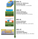
Research progress of NiO/β-Ga₂O₃ heterojunction in the field of power devices by the team of Professor Wang Gang from Sun Yat-sen University​


Recently, the team of Associate Professor Lu Xing and Professor Wang Gang from Sun Yat-sen University summarized the research progress of NiO/β-Ga2O3 heterojunction in the field of power devices, and made a prospect for its future development. The review starts from the construction, characterization and device performance of NiO/β-Ga2O3 heterojunction, and discusses the crystallization properties and energy band structure of NiO/β-Ga2O3 heterojunction prepared by sputtering method and carrier transport characteristics, and introduced NiO/β-Ga2O3 heterogeneous pn junction diodes (HJD), junction barrier Schottky diodes, junction field effect transistors and NiO/β-Ga2O3 based The latest developments in various device structures including heterojunction edge termination structures and super junction (SJ) structures. In addition, the paper also summarizes and looks forward to the key issues in the practical application of NiO/β-Ga2O3 heterojunction, such as material quality, device structure optimization, interface state and device reliability.

1688075577329.png

Please, Log in or Register to view URLs content!
 

tokenanalyst

Brigadier
Registered Member

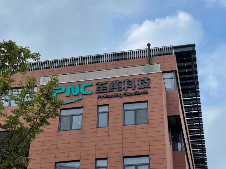
Pure Technology: We have repeated orders for wet cleaning equipment in all 28nm process steps​


1272838652525.55251274298693313.0396.png


According to news from Jiwei.com, recently, some investors asked a question on the investor interaction platform: Your company said that 212 million of the new orders signed in the first quarter of 2.1 billion were process equipment. Does it mean cleaning equipment? Your company's friend Shengmei said that the company's cleaning equipment has covered 90-95% of the cleaning process, and said that new customers accounted for a large proportion of this year's sales. What is the coverage level of your company's cleaning equipment and the trend of new orders for cleaning equipment in the semiconductor industry this year?

Zhipure Technology (603690.SH) stated on the investor interaction platform on June 29 that the company's process equipment covers various types of equipment in the semiconductor field, mainly wet cleaning equipment. The company's wet cleaning equipment has passed verification in all process segments of 28nm and has repeated orders. The company also took the lead in breaking through the monolithic SPM equipment that was originally monopolized by foreign countries.

As of press time, the market value of Zhichun Technology is 13.077 billion yuan, and the stock price is 33.90 yuan per share, an increase of 0.86% from the closing price of the previous day.

Please, Log in or Register to view URLs content!
 

gelgoog

Lieutenant General
Registered Member

China’s semiconductor industry can’t quit German optics​

"When it comes to the optical systems in its lithography machines, SMEE does not tend to source from foreign firms, according to its website. Instead it uses systems from Chinese optics companies like UP Optotech, Focuslight Technologies, and MLOptic Corp. However, recent documents from these firms in turn showed heavy procurements from German and American suppliers."
UP Optotech’s 2021 annual report revealed that the firm’s top supplier wasn’t Chinese, but in fact the German application-specific integrated circuit company iC-Haus. That year, 11.49% of the company’s procurements came from iC-Haus.
So since when is an ASIC "German optics"? Dumbass article. ASICs are chips. And in the case of this German company they seem to make ASICs for sensors and/or mechanical control.

There's plenty more in that article (showing SMEE's suppliers reliant on German, Japanese and American glass polarizers, precision motors, resins, etc. ). So before developing its semiconductor industry, China must develop its lithography industry, and before developing its lithography industry, China must develop its optics, precision positioning instruments, and materials science industries. Interesting reading.
There is no before. Everything must be developed simultaneously. And is being developed simultaneously.
I fully expect the market for things like lenses and materials to continue increasing in China. China already is probably the largest maker of security cameras, and they are also heading towards being the largest maker of cameras for both drones, and smartphones. Not quite the same thing, but China's optics technology has been improving, heck everything has been improving over the past decade.
 
Status
Not open for further replies.
Top