Huatian Technology: Breaking through the barrier of high-end 3D packaging to boost the overall rise of the domestic Chiplet industry
In the post-Moore era, Chiplet has become a bridge for chip manufacturers to enter the next stage of innovation, and provides an excellent technical choice for chip design to break through the PPA ceiling.
To realize the potential of Chiplets, advanced packaging is an indispensable part. The realization of functions such as high-density integration, multi-layer interconnection, low latency and high bandwidth, and good thermal management all require the participation of advanced packaging. In the huge family of advanced packaging, the emerging 3D packaging is gradually revealing its importance to chiplets.
3D packaging is at the right time
Chiplet is an organic combination of independent multifunctional small chips (chiplets), such as processor cores, memory controllers, graphics accelerators, etc. By using 3D packaging technology, these individual components can be stacked together to form a compact 3D structure. The advantages of this 3D integration can provide better performance, energy efficiency and space utilization.
The dynamics of multiple application levels jointly promote the development of 3D packaging. First of all, high-performance computing and processing requirements put forward higher requirements for 3D packaging, providing higher computing density and processing power through multi-chip stacking. Second, the miniaturization and functional enhancement of mobile devices has promoted the application of 3D packaging technology to realize chip stacking and functional integration. Third , the development of the Internet of Things requires the integration of various functional modules, and 3D packaging technology provides a highly integrated and compact design solution. Fourth , the demand for high-speed communication and data processing has promoted the research of short-distance high-density interconnection to improve the efficiency of signal transmission and data processing. At the same time, cost-effectiveness and advances in manufacturing technology are also driving the development of 3D packaging, which reduces costs through modular design and utilization of existing manufacturing processes.
According to the report data of the research institution Research and Markets, the global 3D semiconductor packaging market will be 6.6 billion US dollars in 2020, and the revised scale will reach 14.7 billion US dollars by 2026, with a compound annual growth rate of 14.6%.
Based on different technical paths, 3D packaging also presents various forms, including wire-bonded multilayer chip stacking, package stacking (PoP), and 3D fan-out packaging. Major semiconductor manufacturers have also followed up and continued to innovate in 3D packaging technology. For example, the system integrated packaging technology eSinC SiP developed by Huatian Technology based on the 3D Matrix3D wafer level packaging platform can realize multi-chip high density and high reliability by integrating silicon-based fan-out packaging, bumping technology, TSV technology, C2W and W2W technology.
Dominate the world with silicon-based substrates

The full name of eSinC (Embedded System in Chip) is embedded integrated system-level chip technology, which is a 3D packaging technology launched by Huatian Technology in 2019.
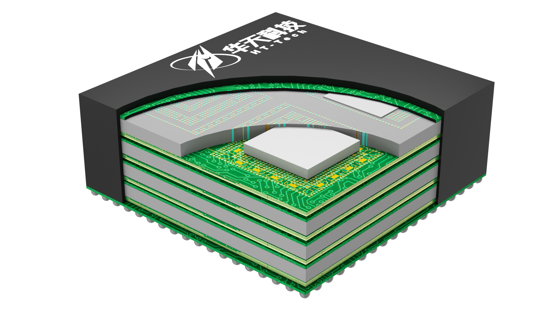
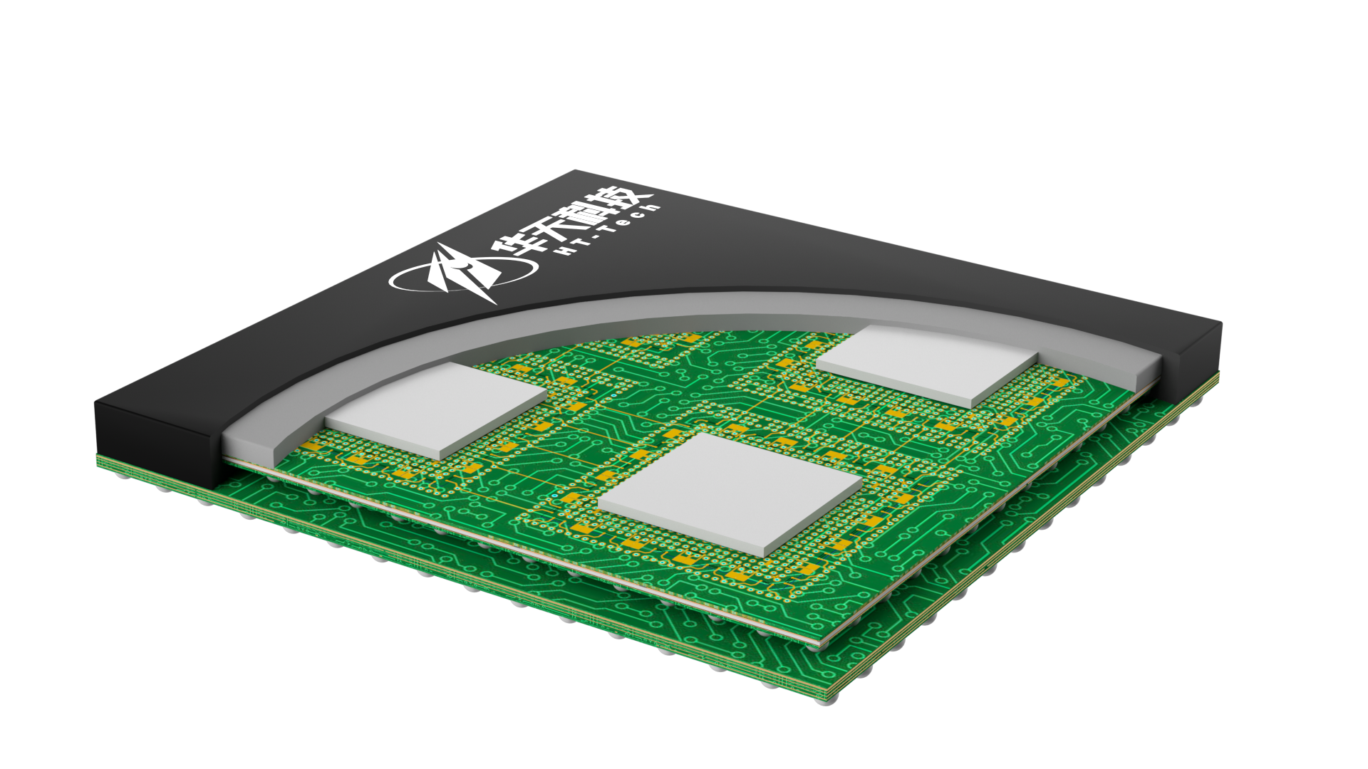
To introduce eSinC technology, it is necessary to mention another technology developed by Huatian Technology, eSiFO (embedded Silicon Fan-out, silicon-based fan-out wafer-level packaging). This technology etches a groove on the silicon substrate, and places the chip with its front facing up and fixes it in the groove. The surface of the chip and the surface of the silicon wafer form a fan-out surface, and multi-layer rewiring is performed on this surface, and lead-out Terminal balls, and finally dicing, separation and packaging.

eSiFO technology can integrate multiple chips together. Compared with traditional packaging, the overall package size is greatly reduced, the interconnection between chips is shorter, and the performance is stronger . On the basis of eSiFO technology, Huatian Technology continued to develop 3D fan-out wafer-level packaging eSinC based on large cavity dry etching, TSV blind holes and temporary bonding technology. This technology uses TSV vias to realize vertical interconnection, which greatly improves interconnection density and integration.
The package size that can be achieved by eSinC can reach up to 40mm×40mm, the bump/pitch size of the flip chip can be as small as 40μm/70μm, and the interconnect TSV aspect ratio can be 5:1. Integrating 8 chips, the overall package thickness is less than 1mm. The target applications of this technology are mainly Al, IoT, 5G and processors and many other fields.
Compared with the existing 3D wafer-level fan-out packaging technology (such as InFo-PoP) on the market, eSinC technology realizes 3D interconnection through high-density via last TSV. Compared with the TMV technology of InFO-PoP, its interconnection density is higher, and the packaging thickness can be selected according to different customer needs, especially in the field of 3D ultra-thin high-density packaging.
The biggest advantage of eSinC lies in replacing the plastic encapsulant with silicon base. With silicon as the carrier, its thermal expansion coefficient, Young's modulus, and thermal conductivity are all better than those of plastic encapsulants, and the silicon carrier is made of the same material as the chip, so the wafer warpage of eSinC will be significantly smaller than that of InFo-PoP, and eSinC products will The heat dissipation performance is significantly better than that of InFo-PoP products.
Mounting a chip on an eSinC wafer or stacking two eSinC wafers becomes a 3D FO SiP packaging technology, which can realize SiP packaging with different structures. Together with TSV and eSiFo, this technology also constitutes Huatian Technology's 3D Matrix wafer packaging platform.
The realization of advanced packaging is inseparable from the support of equipment and materials, and the entire eSinC process is based on numerous localized equipment, such as etching machines, high-precision placement machines, PVD, electroplating machines, exposure machines, bonding machines, etc. The completion has realized the safety and controllability of the supply chain, and also laid a solid foundation for the overall breakthrough of domestic advanced packaging.
Add impetus to the development of domestic Chiplets
At present, the advanced packaging used by Chiplet mainly has the following three forms: one is to directly integrate the system on the organic substrate, the other is to integrate the silicon bridge on the organic substrate, and the third is to use 2.5D packaging technology, such as TSMC’s CoWoS process. These three packaging forms all require organic substrates, because the lack of production capacity of high-end substrates has caused great challenges to packaging factories and formed a high technical threshold.
The advantages of the eSinC process are fully reflected here. Since it does not require an organic substrate, eSinC overcomes the high threshold of the above three packaging forms, so it has become an important solution for packaging factories to realize Chiplet packaging, which is more conducive to the promotion of the entire technology.
In order to adapt to the pace of Chiplet technology development, Huatian Technology has also planned three development goals for eSinC technology. First, as the number of integrated chips continues to increase, the size of a single chip is also increasing, and the package size will gradually increase; second, the aspect ratio of TSV is increasing, and the pitch size is decreasing; third, RDL The line width and line spacing are getting smaller and smaller, and the number of layers will be more and more, in order to cope with the trend of increasing I/O density after the chip is powerful.
In the future, on the basis of this technology, platform technologies such as fine pitch RDL, hybrid bond, and advanced substrates can be further combined to further increase the packaging density and establish a complete Chiplet packaging platform.
The development of independent packaging technology will also greatly stimulate the entire chiplet packaging industry chain in China, especially with localized equipment and localized materials will usher in new development opportunities.
In the context of the increasingly fierce global technological competition and the blockade of key domestic semiconductor technologies, we must develop our independent Chiplet technology and achieve technological innovation. Guided by original technologies such as eSinC, we will further promote key equipment for advanced packaging. , The localization of key materials, change the passive situation of key equipment and key materials relying on imports, and realize the independent control of the supply chain as soon as possible.


