Semiconductor structures and methods of forming them (CN112017948B)
Assignee:
SMIC Integrated Circuit Manufacturing (Shanghai) Co., Ltd.
SMIC Integrated Circuit Manufacturing (Beijing) Co., Ltd.
Abstract
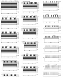
A semiconductor structure and a method for forming the same, the method comprising: providing a substrate, including a first region and a second region, the target pattern pitch formed in the second region is greater than the target pattern pitch formed in the first region; forming a bottom core on the substrate material layer; forming a first core layer on the bottom core material layer; forming a first mask sidewall on the sidewall of the first core layer; forming a second mask side on the sidewall of the first mask sidewall in the second region wall, the second mask sidewall and the first mask sidewall in the second region constitute the third mask sidewall; the first core layer is removed; the first mask sidewall and the third mask sidewall are used as mask patterns The bottom core material layer is formed to form a second core layer; the first mask sidewall and the third mask sidewall are removed; the fourth mask sidewall is formed on the second core layer sidewall; the second core layer is removed; The fourth mask sidewall is a mask patterned substrate, forming a target pattern protruding from the rest of the substrate. The invention satisfies different spacing requirements of target graphics.
The invention relates to a semiconductor structure and a forming method therefore. The method comprises the steps of: providing a substrate, where in the substrate comprises a first area and a second area, and the distance between target patterns formed in the second area is larger than that between target patterns formed in the first area; forming a bottom core material layer on the substrate; forming a first core layer on the bottom core material layer; forming a first mask side wall on the side wall of the first core layer; second mask side wall on the side wall of the first mask side wall in the second region, where in the second mask side wall and the first mask side wall in the second region form a third mask side wall; removing the first core layer;patterning the bottom corematerial layer by taking the first mask side wall and the third mask side wall as masks to form a second core layer; removing the first mask side wall and the third mask side wall; forming a fourth mask side wall on the side wall of the second core layer; removing the second core layer; and patterning the substrate by taking the fourth mask side wall as a mask to form a target pattern protruding out of the remaining substrate. According to the invention, different spacing requirements of the target graph are met.and patterning the substrate by taking the fourth mask side wall as a mask to form a target pattern protruding out of the remaining substrate. According to the invention, different spacing requirements of the target graph are met.and patterning the substrate by taking the fourth mask side wall as a mask to form a target pattern protruding out of the remaining substrate. According to the invention, different spacing requirements of the target graph are met.
It looks like they designed method for its use with synchrotron or SSMB radiation:
HSQ is a silica-based inorganic compound with photosensitivity and high resolution. HSQ, which is usually used for electron beam exposure, is a box-shaped structural unit, and its monomer is a cube-shaped molecule. In each corner, there is an H-Si atom connected to other corner H-Si atoms through O atoms; During the exposure process, when the electron beam deposition energy reaches a certain amount, the Si-H bond in the box-like structural unit can be broken, and the Si atoms with dangling bonds will be connected through O atoms to form a Si-H bond. Si bonds, so as to cross-link each other to form a silicon oxide-like amorphous silicon oxide product SiO x , and the amorphous silicon oxide product SiO x is a three-dimensional network structure, which has good mechanical properties and corrosion resistance , so that it can be retained in the subsequent step of removing the remaining first initial protective layer 114 in the second region II.
Therefore, the first protection layer 115 is formed by using HSQ material and exposing the HSQ material, which has a simple process and low process cost. In this embodiment, electron beams are used to perform the exposure treatment, which is beneficial to save process costs. In other embodiments, according to actual process requirements,
X-rays or EUV (extreme ultraviolet, extreme ultraviolet light) may also be used to perform the exposure treatment.
