Chinese semiconductor industry

Status
Not open for further replies.

hvpc

Junior Member
Registered Member
Nexchip's price/wafer is much higher than Huahong,don't know why is that?

View attachment 112506


View attachment 112507
The Nexchip numbers are in RMB and it’s ASP for 12” whereas HH’s is 8” equivalent ASP.

Nexchip’s 8” equivalent ASP of $600 is just a tad higher than HH’s $581. HH’s wafer mix, having more older nodes drags down its overall ASP number.
 
Last edited:

tonyget

Senior Member
Registered Member
Please, Log in or Register to view URLs content!

Vice Chairman HanZheng visit ASML

https://image.hkhl.hk/f/1024p0/0x0/100/none/1b95760c5bb848f7488ec13027cececa/2023-05/0513028.JPG
 

tphuang

Lieutenant General
Staff member
Super Moderator
VIP Professional
Registered Member
Even more on this
Please, Log in or Register to view URLs content!
This really does seems like a very interesting approach. They first tried this computation in SRAM approach last year on a 22nm process. Now, they are able to generate even more powerful & efficient chip with 12nm process

so there is a well known issue where 60% of time is spent on data transfer and over 90% of power is used in data transfer. So my putting the computation unit inside SRAM (it's not clear how they are doing this), but they claim to greatly reduce # of calls into memory unit and computation unit, making it a lot more efficient. Didn't mission hybrid bonding or anything like this


It's known that computation speed is advancing faster than memory bandwidth. By placing them close together, this just decreases the stale time of the computation unit. Alibaba Damo academy put memory/computation in 1 unit as a top 10 trend in 2023.

Looks like this has been supported by 55 possible customers. From what I can see, this is not limited to autonomous driving. If they scale this up and make it on 7nm process, this could be a very powerful GPGPU

It seems like this is a very new concept, so there is a lot of improvement ahead still

While researching into this, I found this
Please, Log in or Register to view URLs content!
it makes sense to me that SRAM used for caching would have harder time to shrink than your regular logic transistor section, because DRAM also has the same issue with lowest density at 10nm from what I hear.

And there is no way you can build CPU or GPUs without a large cache. As processing needs increase, so does need for accessing larger caching, since it's much faster than DRAM. One of the keys to developing high performing CPU is having a well designed levels of caching.

So if you can't shrink caching at all after 5nm & can barely shrink after 7nm, then at some point, I think you will reach the point of diminishing returns in ever higher cost of packing more logic transistor.

IIRC, @FairAndUnbiased mentioned that as you get to more advanced nodes with higher densities, there is also higher % of dark transistors that can't be accessed. Any link on that, btw?

I could be entirely wrong here, but it seems like once you get to something between 5 and 7nm process, shrinking further & packing more transistors won't get the scale of improvements compared to 28nm to 14nm

So improvements to CPU/GPU performance probably reside in more improved designs like what we see with this Houmo chip and more improved 3D packaging to get memory & logic die closer to each other and to improve the bond between them
 

tphuang

Lieutenant General
Staff member
Super Moderator
VIP Professional
Registered Member
006DKHfbgy1hdwqica5yej30xc0c07eb.jpg
006DKHfbgy1hdwqicn9d7j310g0kmwob.jpg
btw, new patent from Huawei on advanced packaging. I actually don't understand this at all, so I will let you guys figure it out
From Huawei whisper
华为最新公布了一个新专利,半导体封装技术

华为消息正在稳步推进属于自己的半导体体系,从软件到硬件都在紧锣密布的进行中,关键技术和创新技术不断,绕开专利壁垒的也有,所以华为确实很努力在寻求突破美国带来的半导体封锁。
I think what he says here is entirely expected.

Being restricted to 7nm for a couple of years is not ideal, but with improved packaging and software. At least for AI, HPC and EVs, Huawei imo should be competitive here
 

FairAndUnbiased

Brigadier
Registered Member
IIRC, @FairAndUnbiased mentioned that as you get to more advanced nodes with higher densities, there is also higher % of dark transistors that can't be accessed. Any link on that, btw?

I could be entirely wrong here, but it seems like once you get to something between 5 and 7nm process, shrinking further & packing more transistors won't get the scale of improvements compared to 28nm to 14nm

So improvements to CPU/GPU performance probably reside in more improved designs like what we see with this Houmo chip and more improved 3D packaging to get memory & logic die closer to each other and to improve the bond between them
It's well accepted.

Please, Log in or Register to view URLs content!

Please, Log in or Register to view URLs content!

Please, Log in or Register to view URLs content!
 

tokenanalyst

Brigadier
Registered Member
View attachment 112544
View attachment 112545
btw, new patent from Huawei on advanced packaging. I actually don't understand this at all, so I will let you guys figure it out
From Huawei whisper

I think what he says here is entirely expected.

Being restricted to 7nm for a couple of years is not ideal, but with improved packaging and software. At least for AI, HPC and EVs, Huawei imo should be competitive here
This is the description of the patent for more context:

technical field
The present disclosure relates to the field of semiconductor manufacturing for producing low cost and high performance small semiconductor devices. In particular, the present disclosure relates to semiconductor packages and a method for producing such packages, such as molded-in modules and sub-modules.

Background technique
Semiconductor manufacturing continues to improve in order to produce smaller semiconductor devices. Smaller devices typically consume less power, have higher performance, and can be produced more efficiently. Additionally, smaller semiconductor devices have a smaller footprint, which is desirable for smaller end products. Smaller semiconductor die sizes can be achieved by improving front-end processes, resulting in semiconductor dies with smaller, higher density active and passive components. Back-end processes can produce semiconductor device packages with smaller footprints by improving electrical interconnect and packaging materials. In addition to laminate embedding, mold embedding is known as a concept to achieve such optimized or derivative packaging, such as pre-packages or subassemblies. One advantage of mold embedding is the high flexibility with respect to the structure to be embedded. The topography of the substrate, chip and contact elements can be easily embedded in the mold compound, whereas laminate embedding requires cutting these features out of the prepreg material.
However, one disadvantage of current mold embedding is its high production cost, whether it is the galvanic deposition of the studs or the laser drilling of the through-holes required for the reference marks.

Contents of the invention

The present disclosure provides an efficient semiconductor manufacturing solution using die embedding without the disadvantages described above. In particular, an alternative mold embedding solution is provided which achieves cost reduction and provides efficient and reliable manufacturing of semiconductor packages.

The foregoing and other objects are achieved by the features of the embodiments. Further implementation forms are evident from other embodiments, the description and the figures.
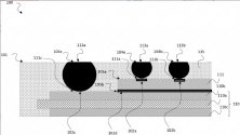
The basic idea of the present disclosure is to use coated Cu (copper) balls for through-die interconnection purposes. For example, these coated Cu spheres can be applied by re-melting the Sn(Tin) coating using laser energy for single sphere placement or by pressureless sintering. The Cu spheres can be partially ground during the fabrication process to achieve the advantages of good thermal and electrical conductivity, and can be directly soldered or sintered on the open Cu surface. Another advantage of partially ground Cu spheres is the ability to provide perfect interconnects to any RDL (Redistribution Layer) deposited on top of the die.
In other words, this disclosure introduces a novel mold embedding technique that uses vertical interconnect elements composed of coated Cu balls; connects the Cu balls to the substrate by welding, diffusion bonding, or sintering; embeds the Cu balls in the mold layer; and connecting the Cu balls to the redistribution layer by partially cutting the Cu balls, for example, milling the mold layer, and depositing the redistribution layer on top of the mold compound.
Accordingly, the present disclosure proposes a novel vertical interconnection technique using, for example, Sn-coated Cu balls as interconnection elements. This novel interconnection technique results in high temperature stability due to the method of diffusing the solder, i.e., no Ni plating or sintering of the balls. Due to the available and proven equipment for ball placement, good manufacturability can be achieved, for example, a high throughput of about 5 balls per second or more can be achieved. Due to the panel production concept (eg 500x600mm), good manufacturability can be achieved. Novel interconnection techniques allow for excellent height compensation (e.g., ±35 μm tolerance for SiC chips), since the contact area is wider after the milling step, eliminating the need for precise focal depths or plating heights, which are ball geometries The advantages. Due to the wider contact area available after the milling step, a low-cost next interconnection step for soldering or sintering leads can be performed.
 

hvpc

Junior Member
Registered Member
That is likely the case for most other Chinese semiconductor companies as well. Not just Nexchip.
Nexchip started out with substantial investment from Powerchip in Taiwan. So of course there was technological transfer from Taiwan as well.

Hopefully they will continue to switch to Chinese wafer and photoresist manufacturers. They already buy at least some wafers and all the gases in China.
Could I ask what you meant by “started out with substantial investment from Powerchip”? Powerchip still has big share of Nexchip after the IPO, no?

Bought Nikon lithography machine

View attachment 112511
Powerchip is known as a “Nikon” fab with Nikon as the tool of record for dry scanners. No surprise Nexchip took after Powerchip’s tool of record.


No they don’t. Nexchip doesn’t have its own maskshop and neither does Powerchip. What you underlined doesn’t equal to Nexchip “make its own mask”

I think it said “mask design”, but what it really means is mask design layout preparation (layout alignment marks, test patterns required by the fab and merchant mask shops, apply OPC to the design, etc.)
 
Status
Not open for further replies.
Top