direct wafer bonding tech allows specialized ICs that are best manufactured on their own processes to be bonded together with a metal interconnect in a single stacked die. example: logic IC used for decoding/encoding memory, and the memory array itself.Can anyone explain to a tech noob like what does this entail?

You are using an out of date browser. It may not display this or other websites correctly.
You should upgrade or use an alternative browser.
You should upgrade or use an alternative browser.
Chinese semiconductor industry
- Thread starter Hendrik_2000
- Start date
- Status
- Not open for further replies.
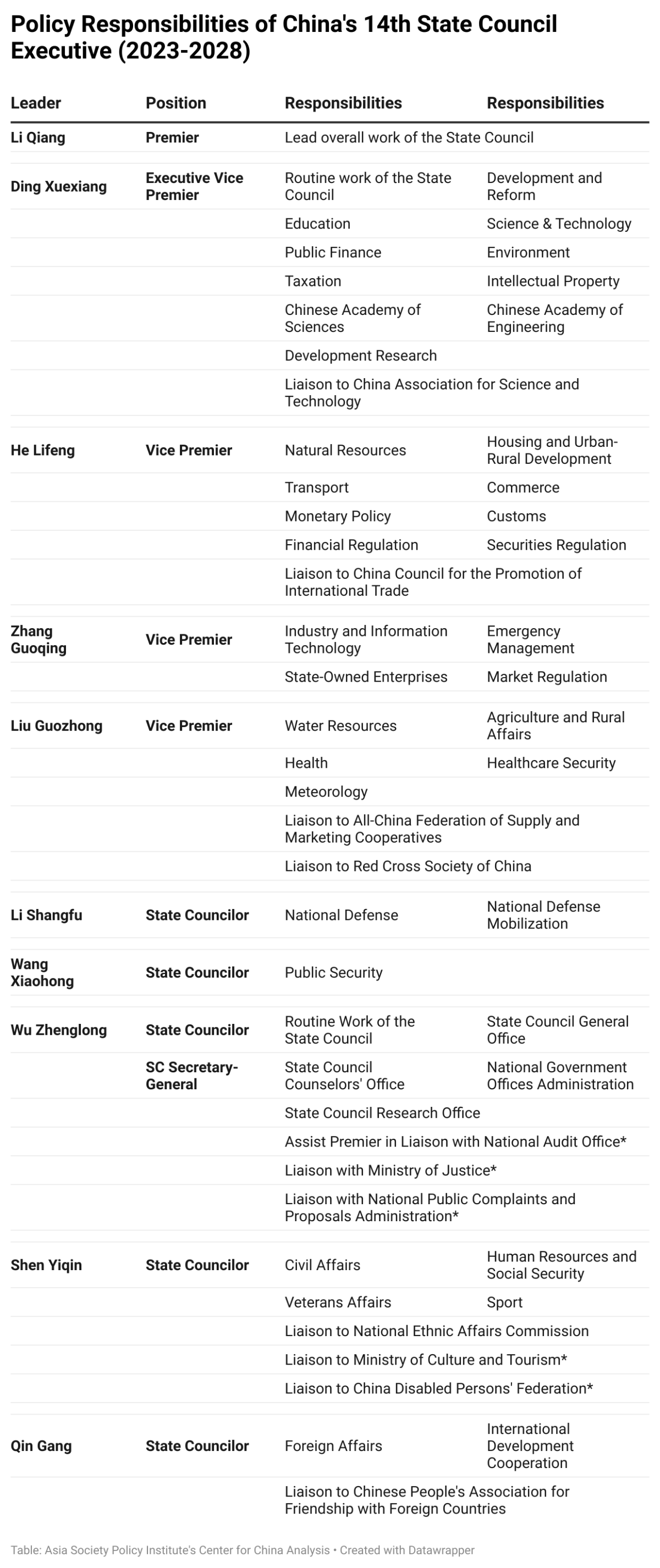
Ding Xuexiang will likely take the lead of the Central Science and Technology Commission from 2023 until 2028. The CPC has upgraded the political importance of science and technology by handing this extremely crucial portfolio to an executive vice premier and politburo standing committee holder instead of a 'normal' vice premier as in previous years. A good sign.
Quite cool, the guy has experience as a material science researcher/engineer. He's also a candidate for the next SecGen.Ding Xuexiang will likely take the lead of the Central Science and Technology Commission from 2023 until 2028. The CPC has upgraded the political importance of science and technology by handing this extremely crucial portfolio to an executive vice premier and politburo standing committee holder instead of a 'normal' vice premier as in previous years. A good sign.
We will see what the man can achieve in five years. He is sixth ranked in the PRC hierarchy. You cannot get closer than that to the inner chamber of the PRC elite. This list is from an Anglophone think tank ''Asia Policy Society Institute''. I do not trust those fuckers but nevertheless a handy list. I have no idea how correct it is but I have noticed Ding attending a climate change meeting in April.Quite cool, the guy has experience as a material science researcher/engineer. He's also a candidate for the next SecGen.
Semiconductor equipment manufacturer Hefei Akeris officially opened
The opening ceremony of Hefei Aikeris Intelligent Equipment Co., Ltd. and the first batch of equipment delivery ceremony of the headquarters base were successfully held.

It is understood that Hefei Aikeris Intelligent Equipment Co., Ltd. is a new main body established by Hunan Aikeris Intelligent Technology Co., Ltd. in Hefei High-tech Zone. With an investment of 100 million yuan, it covers an area of 6,000 square meters. Focusing on the research and development, production and sales of dicing machines for semiconductor packaging and key core functional components, the annual production of 1,000 dicing machines and 2,000 sets of key functional components can be achieved.

Akiris is a national high-tech enterprise. Its products are benchmarked against Japanese DISCO and Tokyo Precision. It provides semiconductor dicing machines and key components with fully independent intellectual property rights, and at the same time exports the overall solution including dicing process and dicing tools to customers. plan. The company's founding team has participated in major national projects such as the 04 major project and the 863 project, and has obtained more than 20 national patents and software copyrights. At present, the performance indicators of the 6-12-inch dicing machine developed by the company are completely comparable to those imported, and it has received bulk orders from leading customers in the semiconductor sensor, optoelectronic devices, discrete devices and other market segments, and has been widely recognized by downstream customers.
full year report from Shanghai Sinyang
Will have that new production base in Hefei that have 2 phases under construction at same time. Total planned capacity of 70k t. Phase 1 equipment is being installed. So expect a lot more sales this year
14nm product is also been mass produced.
so they have everything 14nm and above covered when it comes to dry etching cleaning liquid
Talks about needing to localize
Sounds like Krf photoresist coverage and sample will continue to increase
Arf immersion photoresist development has been smooth. ASML-1900 scanner installed and testing with photoresist has achieved performance that are comparable with target product. No comment here on if it has been validated (again, this is for achievements from 2022).
It's Shanghai factory completed and have annual production of 19k t of different chemical material. Produced 11.8kt last year.目前上海厂区年产能1.9万吨扩充目标已建设完成。报告期内,公司化学品产出1.18万吨,较去年同比增加16.84%,其中超纯化学材料产品产量增长超50%以上。公司合肥第二生产基地项目适时调整,一期二期同时开展建设,合计规划产能7万吨,目前一期已在设备安装调试阶段。
Will have that new production base in Hefei that have 2 phases under construction at same time. Total planned capacity of 70k t. Phase 1 equipment is being installed. So expect a lot more sales this year
cleaning liquid for 28nm dry etching has been mass produced在集成电路制造用清洗液产品方面,28nm干法蚀刻后清洗液产品已规模化量产,14nm技术节点后干法蚀刻后清洗液也已量产并实现销售,公司干法蚀刻后清洗液产品已经实现14nm及以上技术节点全覆盖。本报告期干法蚀刻后清洗液产品销售已超过亿元,广泛应用于逻辑电路、模拟电路、存储器件等晶圆制造领域。其中,铝互连干法蚀刻后清洗液长期受制于国外唯一原材料供应商限制,面对先进制程所需的配套材料亦需国产化的现状,公司经过自主研发攻关,“卡脖子”的关键原材料项目——非羟胺项目报告期内取得重大技术突破,已开发出满足晶圆制造企业要求的无羟胺干法蚀刻后清洗液产品。目前该产品已通过国内主流晶圆制造客户的验证,标志着我司对铝制程清洗技术的理解与研发能力已走在世界前列。
14nm product is also been mass produced.
so they have everything 14nm and above covered when it comes to dry etching cleaning liquid
Talks about needing to localize
mass production of silicon nitride etching solution products for 128-layer and above 192 layer have been achieved and on sale. Getting 100m RMB of sales on this在蚀刻液产品方面,公司紧跟芯片制造技术的发展和行业领先客户的先进制程,持续推进相关产品的研发,进行产品技术能力的储备,新一代更高阶产品的小试技术储备已完成,技术性能达到国际先进水平,未来相关系列产品持续在更多客户端上线验证,进一步扩大应用。目前已量产的应用于128层、192层及以上的氮化硅蚀刻液产品已规模化销售,报告期内实现销售收入超1亿元。
Probably the most important part. I-line & krf photoresist have been sent for validation at over 10 customers and got orders and passed validation. Company's photoresist product continue to improve to satisfy customer process requirements.在光刻胶及研磨液两大类产品方面,报告期内均取得了不同程度的进展和突破。其中,光刻胶研发进展比较顺利,I线、KrF光刻胶已经在超10家客户端提供样品进行测试验证,并取得了部分样品的订单,通过测试验证,公司光刻胶产品工艺性能指标不断优化,以满足客户的工艺需求。此外,部分产品已获得晶圆制造企业小批量连续订单。后续KrF光刻胶的样品测试验证的范围和样品类别还将继续扩大,从而加速产业化目标的实现。ArF浸没式光刻胶的研发进展也比较顺利,ASML-1900光刻机安装调试进度符合预期,安装调试基本结束,公司研发的实验室样品目前取得的数据指标和对标产品大部分接近。
Sounds like Krf photoresist coverage and sample will continue to increase
Arf immersion photoresist development has been smooth. ASML-1900 scanner installed and testing with photoresist has achieved performance that are comparable with target product. No comment here on if it has been validated (again, this is for achievements from 2022).
Company working with Shanghai chemical industrial zone to build production base. In terms of slurry products, the company's chemical mechanical polishing (CMP) technology has matured STI slurry, Poly slurry, and W slurry series products have passed customer tests and entered the stage of mass production公司与上海化学工业区达成建设生产基地的意向,目前正推进项目建设的各项前期工作。在布局的研磨液系列产品方面. 公司的化学机械研磨液(CMP)技术也已有成熟的STI Slurry、Poly slurry,W slurry 系列产品通过客户测试,进入批量化生产阶段。报告期内光刻及研磨两大系列产品实现营业收入超百万元。
Yes, but what about the reported performance? To me it sounds incredible.direct wafer bonding tech allows specialized ICs that are best manufactured on their own processes to be bonded together with a metal interconnect in a single stacked die. example: logic IC used for decoding/encoding memory, and the memory array itself.
“Compared to the CPU-DRAM system, our chip achieves 9.78× speedup. Note that the throughput and memory capacity can be further improved by scaling up the number of hybrid bonding blocks or using more advanced process technologies to serve more complicated recommendation models. In terms of energy efficiency, which is significant in memory-bound applications, our work achieves 184.11QPS/W (QPS – Queries per Second), which outperforms the CPU-DRAM system by 317.43×. In terms of area efficiency, the high-density hybrid bonding improves QPS/mm2 by 660×.” The results were achieved while using a relatively old process node of 55 nm for the logic and were compared with the top-of-the-line Intel Xeon Gold CPU processed at 14 nm.
I am not a SME in chip architecture. But this is how I understand it: the bottleneck isn't in the computational steps per clock cycle anymore but in how fast the processor transfers data from memory.Yes, but what about the reported performance? To me it sounds incredible.
. That means it has 1 Tx and Rx channel, with each Tx channel transmitting data as a sequential digital signal. Example: you want to transmit signal A,B,C,D,E. On a serial connection, your computer then transmits A, B, C, D, E, in order. If you have more than 1 channel, you can write more. This is a linear scaling. For 2 channels, you can read/write to/from DRAM 2x faster. So it can transmit i.e. A1, A2, A3, A4, A5, A6. Then B1, B2, B3, B4, B5, B6.
.
. That's limited by the form factor of the memory stick.
How about stacking those DRAM dies, integrating the DRAM controller straight into your CPU, and reading off the DRAM controller directly with arbitrary channels? 288 pins is pretty big because it has to deal with PCB traces, but you can get thousands of interconnects for IC packages easily. Not SME, ask an actual EE for details.
Funnily enough, Dylan Patel talked about thisI am not a SME in chip architecture. But this is how I understand it: the bottleneck isn't in the computational steps per clock cycle anymore but in how fast the processor transfers data from memory.
. That means it has 1 Tx and Rx channel, with each Tx channel transmitting data as a sequential digital signal. Example: you want to transmit signal A,B,C,D,E. On a serial connection, your computer then transmits A, B, C, D, E, in order. If you have more than 1 channel, you can write more. This is a linear scaling. For 2 channels, you can read/write to/from DRAM 2x faster. So it can transmit i.e. A1, A2, A3, A4, A5, A6. Then B1, B2, B3, B4, B5, B6.
.
Some things that slow it down: The signal from the Intel Xeon Gold has to travel along the wires in the PCB, which introduces a time delay. Traveling outside the chip introduces EM noise, such as RF noise from external RF signals picked up by PCB traces acting as antenna, etc. To remove this noise, you introduce noise reducing measures like filters - but that makes it just a little bit slower.
Now instead of 6 channels along a PCB trace, you wafer bond the DRAM directly to your CPU. Now there's 0 travel time delay and reduced noise. But the big one is, you can have arbitrary channels:
. That's limited by the form factor of the memory stick.
How about stacking those DRAM dies, integrating the DRAM controller straight into your CPU, and reading off the DRAM controller directly with arbitrary channels? 288 pins is pretty big because it has to deal with PCB traces, but you can get thousands of interconnects for IC packages easily. Even a simple macroscopic ball-grid array (BGA) can get you 2400 pins, so what about lithographically defined interconnects? Maybe 2.88 million?
Even with heavy optimizations from leading researchers, 60% FLOPS utilization is considered a very high utilization rate for large language model training. The rest of the time is overhead, idle time spent waiting for data from another calculation/memory, or recomputing results just in time to reduce memory bottlenecks.
From the current generation A100 to the next generation H100, the FLOPS grow by more than 6X, but memory bandwidth only grows by 1.65x. This has led to many fears of low utilization for H100. The A100 to get around the memory wall, and more will need to be implemented with the H100.
While capacity is a significant bottleneck, it is intimately tied to the other major bottleneck, bandwidth. Increased memory bandwidth is generally obtained through parallelism. While standard DRAM is only a few dollars per GB today, to get the massive bandwidth machine learning requires, Nvidia uses HBM memory, a device comprised of HBM is in the $10 to $20 a GB range, including packaging and yield costs.
So from what I can see, if you customize your AI chip and stack the necessary components together and allow direct I/O between your logic die (doesn't have to be a CPU) and DRAM, your DRAM can be relaly fast. And then if you can increase the bandwidth between DRAM and your GPGPU, it can have better performance so the GPU cycles are not just wasted being idle. There is a reason it's called general purpose GPU, it's designed to handle different scenarios.
If you have a custom design focused on specific applications like AIGC, then you can design your 3D chip & software in a way that maximizes the resources it has.
btw, HBM is talked a lot. Does anyone know if CXMT is designing HBM type of memory? Or maybe YMTC?
latest comment from ASML, this is getting interesting
Doesn't seem like the people at the top are listening.
If you read this the first time, it sounds quite optimistic. But then you compare this to what ASML said a couple of years ago. Now, it's a plea to Dutch gov't to keep market access open. It is absolutely essential that we get to keep having market access to China!Wennink said at ASML's annual meeting on Wednesday that he was not worried about rivals in Japan, the U.S. or China being close to building cutting edge commercial lithography products.
"But it can happen of course, so it is absolutely essential that we get to keep having market acess to China", which is the largest market for computer chips globally. "Market access is as important to us as it is to our Chinese customers," he said.
Doesn't seem like the people at the top are listening.
I believe this applies to a company starting with letter B. Yes, there are many semi fabs in construciton for the NEVs.He said one unnamed carmaker in mainland China, ASML's third market after Taiwan and South Korea, plans to make so many electric vehicles in the next three years that it would require "six or seven full-fledged logic semicondcutor factories" that haven't yet been built.
- Status
- Not open for further replies.