Chinese semiconductor industry

Status
Not open for further replies.

tphuang

Lieutenant General
Staff member
Super Moderator
VIP Professional
Registered Member
So how come Caijing quotes the Huawei executive that they made tools "above 14nm" in collaboration with Chinese EDA companies and Reuters spins it that they have made tools for 14nm? I mean, Reuters is usually better than this.

"above 14nm" means no FinFET. It is probably only for planar transistors up to 28nm and the like. Which is what makes sense for Huawei, since they have like a single factory in the whole of China which can make FinFET for them right now. While there are many factories which can make planar transistor processes.
btw, the Huawei Whisper commented on this. It definately includes 14nm process. The next step is 10nm. No reason to include 14nm in his phrasing if it cannot do 12/14nm process of SMIC.

At this point, I'm really curious what's left to replace American suppliers in the 14nm process for SMIC. And how close AMEC is able to replace Lam products there.
 

spaceship9876

New Member
Registered Member
FinFET use started in 22 nm node for Intel. Then TSMC and samsung further upgraded their 28 nm processes and called those 20 nm despite them still having planar transistors and lower performances than Intel 22 nm. Then they introduced a FinFET node finally. They were called 16 nm but their performances were lower than Intel 22 nm in many aspects. Their 12 nm were also just upgraded versions of their 16 nm processes. Intel's 14 nm was a full node development over their 22 nm. This is how we ended up with Intel 14 nm outperforming other's 10 nm processes.

To sum up: The territory FinFET starts becoming a net benefit starts way above 14 nm.
globalfoundaries has their 22nm SOI process too. The problem with finfet is the chip design costs are much higher.
 

tokenanalyst

Brigadier
Registered Member

Shanghai Shengxi intends to supply 28 sets of evaporation source equipment to Xiamen Tianma Display, with a contract value of about 129 million yuan.​


Jiweiwang news, on the evening of March 24, Allied announced that Shanghai Shengxi Optoelectronics Technology Co., Ltd. (hereinafter referred to as "Shanghai Shengxi"), a wholly-owned subsidiary of the company, provided 28 sets of lines to Xiamen Tianma Display Technology Co., Ltd. Evaporation source equipment, the contract value is 128,707,000 yuan (tax included).

Please, Log in or Register to view URLs content!
 

tokenanalyst

Brigadier
Registered Member

Huawei disclosed the progress of EDA for the first time: some key links of independent replacement have been overcome.​

According to the report of Caijing Eleven, on February 28, Xu Zhijun, Huawei's rotating chairman, disclosed the latest progress of Huawei's software design tools for the first time at the Huawei Summary and Commendation Meeting.

Xu Zhijun pointed out that Huawei has completed the localization of EDA tools above 14nm in the chip field, and will complete comprehensive verification this year; Huawei's three R&D production lines for hard and soft cores (hardware development, software development, and chip development) have currently completed software/hardware development. 78 software tools They can basically guarantee the continuity of R&D operations. The report pointed out that Huawei should be the first in China to simultaneously develop a full set of software design tools on the three R&D production lines of hardware, software and chip development.

Please, Log in or Register to view URLs content!
 

siegecrossbow

General
Staff member
Super Moderator

Huawei disclosed the progress of EDA for the first time: some key links of independent replacement have been overcome.​

According to the report of Caijing Eleven, on February 28, Xu Zhijun, Huawei's rotating chairman, disclosed the latest progress of Huawei's software design tools for the first time at the Huawei Summary and Commendation Meeting.

Xu Zhijun pointed out that Huawei has completed the localization of EDA tools above 14nm in the chip field, and will complete comprehensive verification this year; Huawei's three R&D production lines for hard and soft cores (hardware development, software development, and chip development) have currently completed software/hardware development. 78 software tools They can basically guarantee the continuity of R&D operations. The report pointed out that Huawei should be the first in China to simultaneously develop a full set of software design tools on the three R&D production lines of hardware, software and chip development.

Please, Log in or Register to view URLs content!

ykxMKKO.gif


All joking aside other Chinese firms really need to get their act together. Recently Huawei CEO complained without naming names that many Chinese cellphone makers used Huawei proprietary designs without paying.
 

tokenanalyst

Brigadier
Registered Member

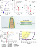
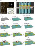
School of Electronics, Peking University develops two-dimensional transistor with speed exceeding silicon limit.​

the research team of Professor Peng Lianmao and Researcher Qiu Chenguang from the School of Electronics, Peking University has prepared a 10nm ultra-short channel ballistic two-dimensional indium selenide transistor, which for the first time made the actual performance of the two-dimensional transistor exceed that of Intel's commercial 10nm node silicon-based Fin transistor , and reduce the operating voltage of the two-dimensional transistor to 0.5 V, which is also the fastest and lowest energy consumption two-dimensional semiconductor transistor in the world so far. The relevant research results are titled "Ballistic two-dimensional InSe transistors.

This work has achieved three technological innovations: using three layers of indium selenide with high carrier thermal velocity (smaller effective mass) as the channel, and achieving a room temperature ballistic rate as high as 83%, which is the highest value of field effect transistors at present. Much higher than the ballistic rate of silicon-based transistors (less than 60%); solved the problem of growing ultra-thin oxide layers on the surface of two-dimensional materials, prepared 2.6 nanometer ultra-thin double-gate hafnium oxide, and increased the device transconductance to 6 mS Micron, an order of magnitude more than all two-dimensional devices; pioneered doping-induced two-dimensional phase transition technology to overcome the international problem of gold-half contacts in the field of two-dimensional devices, refresh the total resistance to 124 ohm microns, and meet the requirements of future nodes of integrated circuits for transistors Resistor Requirements (220 ohms • microns).

1679659597594.png1679659677145.png


Please, Log in or Register to view URLs content!
 
Status
Not open for further replies.
Top