Chinese semiconductor industry

Status
Not open for further replies.

Weaasel

Senior Member
Registered Member
Maybe we will finally see it this week.

What an interesting day. Confirmation of:
1) SMEE winning lithography orders (likely for DUV)
2) Huawei getting domestic produced 5G SoC chiplet from SMIC
3) SMIC 7nm process getting breakthrough
4) SMIC 12/14nm process seeing high yield
5) Big fund giving a lot of money to domestic chip industry.
Really. That sounds like very good news. I hope it happens at some time this year for sure, sooner rather than later, hopefully...

If all that happens, the Americans will - ... Just imagine their reaction...
 

tokenanalyst

Brigadier
Registered Member

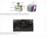
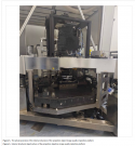
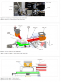
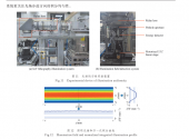
Analysis of Displacement Measurement Error in Distortion Detection of Lithographic Projection Objective Lens​

  • Institute of Optoelectronic Technology, Chinese Academy of Sciences State Key Laboratory of Optical Technology for Microfabrication, Chengdu 610209, Sichuan
Abstract:
In the distortion detection of the lithography projection objective, the displacement measurement error is one of the important error sources. Depth analysis of the error sources and reduction of the error terms can improve the distortion detection accuracy. stage, this paper analyzes the displacement measurement error of the image quality detection stage when the Shack-Hartmann wavefront sensor is used to detect the distortion of the projection objective. In this paper, a set of image quality detection platform is taken as an example to analyze the displacement measurement error in the distortion detection of the projection objective, and the image quality detection platform is used to measure the distortion of a projection objective. The distortion detection result is about 80 nm,In which the displacement measurement error of the image quality detection platform will bring about an uncertainty of about 22 nm to the distortion detection result.

1678817431082.png1678817486263.png
1678817538970.png1678817626795.png


Please, Log in or Register to view URLs content!
 

tphuang

Lieutenant General
Staff member
Super Moderator
VIP Professional
Registered Member
Big news, CETC 46th Institute has now prepared China's first 6-inch Gallium Oxide wafer
Please, Log in or Register to view URLs content!
This was first achieved a year ago by the Japanese
Please, Log in or Register to view URLs content!

Keep in mind that America considered it so sensitive that Gallium Oxide tech was restricted from China last August
Please, Log in or Register to view URLs content!

There are wide applications in both military and commercial fields, but I'd imagine military usage is more applicable right now. It would most likely allow for more powerful radar than the current GaN AESA radar. It could also be used in other applications that require operating under high temperature and voltage environment.
This is almost hard to believe

Please, Log in or Register to view URLs content!
They are up to 8 inch wafers now. It only took 2 weeks.
This is from a university I've never heard of 西安邮电大学.

I haven't read anyone outside of China with 8 inch Ga2O3 wafers
 
Last edited:

FairAndUnbiased

Brigadier
Registered Member
This is almost hard to believe

Please, Log in or Register to view URLs content!
They are up to 8 inch wafers now. It only took 2 weeks.
This is from a university I've never heard of 西安邮电大学.

I haven't read anyone outside of China with 8 inch Ga2O3 wafers
It's actually a pretty high ranked university in China, originally made to build out China's recovering telecom network back in the 1950s. It's not a surprise to me.
 

latenlazy

Brigadier
So big fund invested 204.1B RMB in 40 companies. Chipmaking represented 67%, designing 17%, packaging 10% and tools/material just 6%
Major investment seem to be at YMTC and SMIC's new fabs.
Also quite a bit with CXMT, CR Micro, Silan & FullSemi

View attachment 109144
This funding split actually makes some sense. If you fund the fabs they can define who to fund in terms of equipment. You're still providing passive financial support to equipment makers, but using their customers as your filter rather than judgments directly from a executive finance desk far removed from the specifics.
 

latenlazy

Brigadier

Nanda Optoelectronics: We are stepping up the verification work of ArF photoresist products​


1468133890678.353.png


According to news from Jiwei.com, recently, some investors asked a question on the investor interaction platform: Excuse me, teacher, the verification time for the 28nm part of photoresist is so long, is your company wasting time?

Nanda Optoelectronics (300346.SZ) stated on the investor interaction platform on March 14 that the company is stepping up the product verification of ArF photoresist.

As of press time, the market value of Nanda Optoelectronics is 19.426 billion yuan, and the stock price is 35.73 yuan per share, up 2.94% from the closing price of the previous day.
"Give us more money and we'll give you more testing man-hours".
 

latenlazy

Brigadier
It's actually a pretty high ranked university in China, originally made to build out China's recovering telecom network back in the 1950s. It's not a surprise to me.
China's STEM focused "middle tiers" are more like specific departments at MIT and CalTech than they are like the same departments at a US middle tier like Florida State. Not very broad in the fields they support but extremely deep.
 
Status
Not open for further replies.
Top