You are using an out of date browser. It may not display this or other websites correctly.
You should upgrade or use an alternative browser.
You should upgrade or use an alternative browser.
Chinese semiconductor industry
- Thread starter Hendrik_2000
- Start date
- Status
- Not open for further replies.
How about the performance?, comparable to what Intel i5 generation? 7th or 8th ?
Perhaps even i5 7th generation is good enough for most users in the office
All the prior zhaoxin core performance were in the 2 to 4th generation category. Still good enough for office type work if running linux with sufficent ram and ssd.
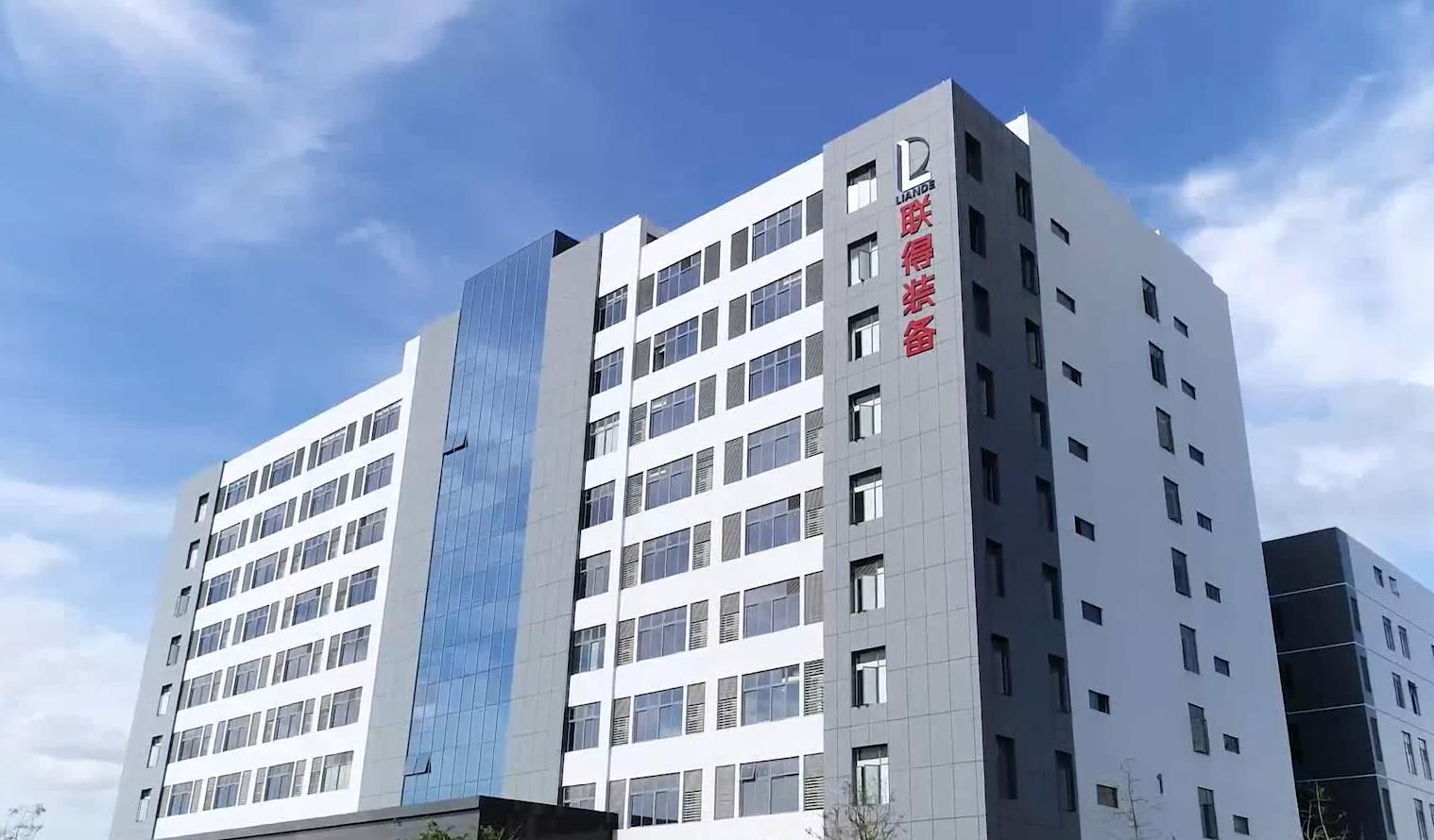
Liande Equipment: Semiconductor die-bonding equipment has entered the mass production stage for customers

According to news from Jiwei.com, recently, an investor asked a question on the investor interaction platform: Is the company's semiconductor die-bonding machine already in mass production, and which customers can you introduce?
Liande Equipment (300545.SZ) stated on the investor interaction platform on March 14 that the company's semiconductor die-bonding equipment has now entered the stage of mass production for customers.
As of press time, the market value of Liande Equipment was 3.484 billion yuan, and the stock price was 19.60 yuan per share, an increase of 1.55% from the closing price of the previous day.
Core Technology Releases CAPiC Die and Advanced Packaging Technology Platform
The innovative achievements of CAPiC die and advanced packaging technology platform mainly include six core packaging technologies, high-density rewiring fan-out structure ( FOCT-R ), high-density through-silicon via fan-out structure ( FOCT-S ), rewiring and silicon Embedded substrate fan-out structure ( SETiS/RETiS ), stacked chip fan-out structure ( TMV-POP ), glass-based fan-out structure ( TGV-POP ), resin / dry film fan-out structure ( eWLB-F/eWLB- M ). This release embodies the strong technical strength and innovation ability of the Advanced Packaging Technology Research Institute of Sintech.
In recent years, the Sintech Research Institute team has focused on the development of Chiplet -related technologies, striving to provide customers with more and better advanced packaging technology solutions, especially through high-density wafer-level RDL integration to reduce the number of substrate design layers , and even achieve the role of replacing the substrate.
Zhang Zhong, vice president of technology of Xinde Technology, gave a detailed introduction to the six major packaging technologies of CAPiC die and advanced packaging technology platform:
1 ) FOCT-R ( FANOUT Connected Tech-RDL ) , mainly used in data centers , server CPUs , computing AI, IOT chips, realizes the interconnection between homogeneous and heterogeneous chips, and can integrate two substrates with different characteristics : A substrate with a high number of layers, a more precise rewiring interposer ( RDL Interposer ), can further realize a larger 2.5D package, and reduce the number of substrate layers. Using redistribution and bump technology, the minimum line width of 2 μm and the wiring of 2um spacing are realized. At the same time, Sintech launched single-chip HPFO technology, using Interposer to effectively reduce the number of substrate manufacturing layers.
2 ) FOCT-S (Fanout Connected Tech- S), dedicated to high-performance computing ( HPC ), artificial intelligence ( AI ), data centers and network products that require high-performance and large-area packaging technology, using silicon transfer boards ( Si Interposer ), which can achieve higher precision ( <1um line width and spacing) rewiring layer, achieve higher density connections, provide higher performance, and give full play to the advantages and characteristics of 2.5D packaging eWLB-M, the main application For the fan-out packaging of medium and large chips , the package size can be around 8x8~15x15mm . Using rewiring and bump technology, the chip can be directly connected to the chip, reducing the thickness, reducing the connection loss, reducing the cost, and cost-effective. Applied to millimeter wave, radio frequency and wireless chip packaging, processor and baseband chip packaging;
3 ) SETiS/RETiS ( Silicon Embeded Tech in Substrate/ RDL Embeded Tech in Substrate ) , an embedded multi-chip interconnect bridge, can realize the interconnection of heterogeneous and homogeneous chips, and the cost is lower. The realization includes CPU , graphics card, memory , IO and other communication among multiple chips, by embedding the rewiring layer interposer ( RDL Interposer ) into the substrate, the communication efficiency between chips can be improved, the loss can be reduced, and the substrate can be reduced without increasing the thickness of the package. Design difficulty and number of layers.
4 ) TMV-POP is mainly used in high computing power packaging. After interconnecting homogeneous or heterogeneous chips through the rewiring adapter board, the interconnection part is introduced into the back of the package through high copper pillars and plastic encapsulants. Lead out the bumps and interconnect with another package again, realize the interconnection between the package and the package without increasing the package plane size, provide performance, and give full play to the advantages of different packages.
5 ) TGV-POP, mainly used in radio frequency chip packaging, has the advantages of high density, low warpage ( CTE match ), high reliability, low loss factor, low chip offset, low warpage, etc. The package uses glass The insulator material greatly reduces the substrate loss and parasitic effect, ensures the integrity of the transmission signal, rewiring on the glass, transfers the bumps and on this basis, the package interconnection between the chip and the chip fully meets the high frequency signal transmission requirements;
6 ) eWLB-F& eWLB-M, mainly used in the fan-out packaging of small chips , the package size can be around 0.6x0.6~15X15mm , using refined ABF film and wafer-level molding solutions, and then wiring And bump technology, the chip is packaged and protected most efficiently, and multiple chips can also be interconnected to achieve the smallest package size, reduce costs, and cost-effective. It can be used for analog chips, audio playback, voltage protection and other chips. This solution can Effectively replace part of the substrate manufacturing requirements and realize the transformation from FCCSP to FANOUT-CSP .
Maybe we will finally see it this week.
What an interesting day. Confirmation of:
1) SMEE winning lithography orders (likely for DUV)
2) Huawei getting domestic produced 5G SoC chiplet from SMIC
3) SMIC 7nm process getting breakthrough
4) SMIC 12/14nm process seeing high yield
5) Big fund giving a lot of money to domestic chip industry.
It looks like SMEE's winning bid #0613-224022215757 is for two laser annealing equipment (not litho):
| 序号 | 产品名称 | 数量 | 简要技术规格 | 备注 |
| 1 | 晶圆激光退火设备 | 2 | 详见招标文件第八章 |
晶圆激光退火设备 (translation w/ GoogleTranslate): Wafer laser annealing equipment
Last edited:
Nanda Optoelectronics: We are stepping up the verification work of ArF photoresist products

According to news from Jiwei.com, recently, some investors asked a question on the investor interaction platform: Excuse me, teacher, the verification time for the 28nm part of photoresist is so long, is your company wasting time?
Nanda Optoelectronics (300346.SZ) stated on the investor interaction platform on March 14 that the company is stepping up the product verification of ArF photoresist.
As of press time, the market value of Nanda Optoelectronics is 19.426 billion yuan, and the stock price is 35.73 yuan per share, up 2.94% from the closing price of the previous day.
The fab investments will go in part as sales to domestic corporations. Also must note that the more downstream (closer to customers) a market is, the bigger the market must be. Upstream markets (equipment makers) cannot make more total revenue than downstream markets (equipment users) otherwise the revenue of the downstream markets drops to 0 and the market collapses, or more commonly, the downstream markets raise prices to pass the price increase to their customers. Upstream companies can have higher margins but not sales. Usually, size of equipment companies is ~10-20% the size of similar market position semiconductor fabs. The electronics industry is then itself bigger than the semiconductor industry, as everyone will charge higher prices.So big fund invested 204.1B RMB in 40 companies. Chipmaking represented 67%, designing 17%, packaging 10% and tools/material just 6%
Major investment seem to be at YMTC and SMIC's new fabs.
Also quite a bit with CXMT, CR Micro, Silan & FullSemi
View attachment 109144
1:10 direct investment between tools and fabs isn't too out of the ordinary.
Wanrun Co., Ltd.: Photoacid generator has achieved pilot product supply
Recently, some investors asked on the investor interaction platform: to what extent has the photoresist monomer and photoresist resin market been promoted? How many partners do you have?
Wanrun Co., Ltd. (002643.SZ) stated on the investor interaction platform on March 14 that the company’s current related products in the field of semiconductor manufacturing materials mainly include photoresist monomers and photoresist resins, and cleaning agent additive materials in semiconductor manufacturing processes. , and related products have been supplied normally. The company's photoresist monomer and photoresist resin product categories and production technologies for semiconductors cover most of the main products; at the same time, in terms of semiconductor photoresist finished materials, we are also ready to accept production customization business. In addition, the photoacid generator developed by the company has achieved pilot product supply. The company's "65 tons of photoresist resin series product project per year" has basically met the conditions for the production of qualified products, and will continue to optimize in the future, and then start trial production, and strive to put it into use as soon as possible. At present, the company has cooperated with more than 10 domestic and foreign customers in the field of semiconductor manufacturing materials. At the same time, the company continues to actively develop new products and expand more domestic and foreign customers. The company hopes to develop into a solid backing for the global semiconductor manufacturing material industry through efforts.
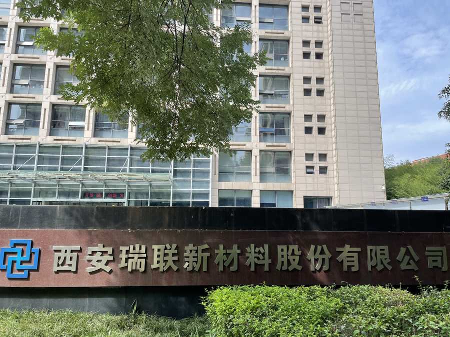
Ruilian New Materials: Some ArF photoresist monomer products have been mass-produced

According to news from Jiwei.com, recently, some investors asked on the investor interaction platform: What level of monomer is the company's photoresist monomer? Is the monomer of arf under development?
Ruilian New Materials (688550.SH) stated on the investor interaction platform on March 14 that the photoresist monomers developed by the company involve ArF photoresist and KrF photoresist, and some of the ArF photoresist monomer products have been measured. Produce.
As of press time, the market value of Ruilian New Materials is 4.942 billion yuan, and the stock price is 50.22 yuan per share, down 0.93% from the closing price of the previous day.
Investors are going ballistic with photoresists companies in China.
So what is going on with photoresists? I remember someone saying that there was a company providing 5,000 tons of arf photoresist in China.
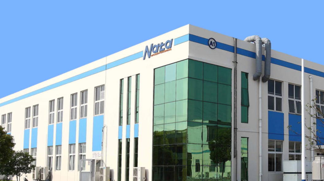
It definitely wasn't Nata, but are there any other companies which provide photoresists?
EDIT: I found what I was referring to.
So essentially there isn't really any substantial arf photoresist production capacity as of right now? We're all just waiting for it to be fully validated and production to spool up?
It definitely wasn't Nata, but are there any other companies which provide photoresists?
EDIT: I found what I was referring to.
Chinese semiconductor industry
Way too optimistic. I am OK if we will see China running a EUV prototype by 2027. From there commercialization will take a few more years. For parity with ASML, 2040 is more realistic. Thank you sir, coming from you I stand corrected. :)
www.sinodefenceforum.com
From what I can figure out, Arf is basically ready at Sinyang. There is a long validation process, but they have already started producing it. If YMTC really gets cut off from ARF photoresist, Sinyang can probably supply them. Worst case scenario is that yield is terrible for a while.
The bigger concern is capacity. They are talking about a 3rd 500t photoresist factory. Fine, but is that going to be enough to supply all of China's advanced process? Let's be optimistic and say Sinyang have 1500t of capacity by 2024 & other companies have 500t. And let's say they don't have to worry about iLine being cut off. Even if we are being generous and say they will have 500t of Krf and 500t of Arf, that still will barely cover need of YMTC, CXMT & SMSC fabs (or maybe not even).
So essentially there isn't really any substantial arf photoresist production capacity as of right now? We're all just waiting for it to be fully validated and production to spool up?
Last edited:
That makes sense. The upstream market probably just needs low interest rate loans to get they factories going. They need to setup policies to encourage fabs to buy from domestic suppliers and work with them. I assume that's the point of these investment + ownership stakes in them.The fab investments will go in part as sales to domestic corporations. Also must note that the more downstream (closer to customers) a market is, the bigger the market must be. Upstream markets (equipment makers) cannot make more total revenue than downstream markets (equipment users) otherwise the revenue of the downstream markets drops to 0 and the market collapses, or more commonly, the downstream markets raise prices to pass the price increase to their customers. Upstream companies can have higher margins but not sales. Usually, size of equipment companies is ~10-20% the size of similar market position semiconductor fabs. The electronics industry is then itself bigger than the semiconductor industry, as everyone will charge higher prices.
1:10 direct investment between tools and fabs isn't too out of the ordinary.
Yes, a lot of updates from both photoresist companies themselves and the upstream suppliers.Wanrun Co., Ltd.: Photoacid generator has achieved pilot product supply
Recently, some investors asked on the investor interaction platform: to what extent has the photoresist monomer and photoresist resin market been promoted? How many partners do you have?
Wanrun Co., Ltd. (002643.SZ) stated on the investor interaction platform on March 14 that the company’s current related products in the field of semiconductor manufacturing materials mainly include photoresist monomers and photoresist resins, and cleaning agent additive materials in semiconductor manufacturing processes. , and related products have been supplied normally. The company's photoresist monomer and photoresist resin product categories and production technologies for semiconductors cover most of the main products; at the same time, in terms of semiconductor photoresist finished materials, we are also ready to accept production customization business. In addition, the photoacid generator developed by the company has achieved pilot product supply. The company's "65 tons of photoresist resin series product project per year" has basically met the conditions for the production of qualified products, and will continue to optimize in the future, and then start trial production, and strive to put it into use as soon as possible. At present, the company has cooperated with more than 10 domestic and foreign customers in the field of semiconductor manufacturing materials. At the same time, the company continues to actively develop new products and expand more domestic and foreign customers. The company hopes to develop into a solid backing for the global semiconductor manufacturing material industry through efforts.
Ruilian New Materials: Some ArF photoresist monomer products have been mass-produced

According to news from Jiwei.com, recently, some investors asked on the investor interaction platform: What level of monomer is the company's photoresist monomer? Is the monomer of arf under development?
Ruilian New Materials (688550.SH) stated on the investor interaction platform on March 14 that the photoresist monomers developed by the company involve ArF photoresist and KrF photoresist, and some of the ArF photoresist monomer products have been measured. Produce.
As of press time, the market value of Ruilian New Materials is 4.942 billion yuan, and the stock price is 50.22 yuan per share, down 0.93% from the closing price of the previous day.
Investors are going ballistic with photoresists companies in China.
I read the entire Nata Q&A for the past few days. it's really embarrassing. They've achieved the least and talked the most.
well, there isn't 5000 ton of ARF Photoresist. I can assure you that. If they get 500t in the next year, it would be pretty good. medium term, getting 5000t of KRF/ARF/iLine photoresist between all the manufacturers is certainly doable.So what is going on with photoresists? I remember someone saying that there was a company providing 5,000 tons of arf photoresist in China.
It definitely wasn't Nata, but are there any other companies which provide photoresists?
EDIT: I found what I was referring to.
Chinese semiconductor industry
Way too optimistic. I am OK if we will see China running a EUV prototype by 2027. From there commercialization will take a few more years. For parity with ASML, 2040 is more realistic. Thank you sir, coming from you I stand corrected. :)www.sinodefenceforum.com
So essentially there isn't really any substantial arf photoresist production capacity as of right now? We're all just waiting for it to be fully validated and production to spool up?
- Status
- Not open for further replies.
