Chris Mack series on Nanofabrication are also pretty good.No, I refer to the change of photoresist reaction with the dose of light absorbed.
Photoresist does not change its structure linearly with the light dose it receives, but until a given threshold it does nothing and then, if the light dose is just a bit more, suddenly changes it's chemical structure. So that while the projected image is smooth and changes gradually due to diffraction limits, the impressed line on the photoresist, and after developing and etching on the wafer, is way much sharper.
All this is well explained in this video:
BTW all this YouTube series by Zeiss (the historical optical subsystem supplier of ASML) on lithography is very instructive to get a good idea of how lithography works.
You are using an out of date browser. It may not display this or other websites correctly.
You should upgrade or use an alternative browser.
You should upgrade or use an alternative browser.
Chinese semiconductor industry
- Thread starter Hendrik_2000
- Start date
- Status
- Not open for further replies.
Among the above-mentioned 331 pieces of equipment won by semiconductor equipment manufacturers in January 2023, domestic equipment manufacturers won a total of 248 pieces of equipment, accounting for as high as 74.92%.
This is why so difficult to determine what "independence" means, China domestic equipment companies have capture 73% of all bidding purchases, give or take depending on how much of the direct purchases are domestic.
Taking into account installed tools foreign companies still dominate because the Chinese are not going to throw those to the sea but in new equipment the BIS export controls may have flipped the US sales share monopoly in favor of Chinese and non US companies.
Sophon maybe?Sophgo is a subsidiary of Bitmain. Have alot of resource ...ahem...money
anyway, this seems to be a very exciting development for China's RISC-V community. Here is the infamous
From算能公司研制的全球首款量产64核RISC-V处理器在2月25日的2022年度中国开放指令生态(RISC-V))联盟大会上正式亮相!
算能公司陆吉年在报告中介绍了三款产品:
① 已经量产的RISC-V 64cores 高性能处理器SG2042(算能科技)
② 将于4月发售的搭载SG2042的手提箱式开发者工作站(万莫斯)
③ 将于6月发售的搭载4颗SG2042芯片的1U高密度计算型服务器(澎峰科技&西研院)
→ 感想:我在现场听了这个报告,很是振奋人心。正如报告中所言,这几款产品能推出,离不开整个生态的支持,从主板设计到定制机箱,从BIOS到操作系统,从编译器到数学库……这是整个RISC-V系统栈不同层的爱好者们协作的成果,而且通过这个RISC-V 64核处理器项目把国内在不同层次的顶尖技术大牛们都汇聚起来了。这群RISC-V爱好者们经常讨论和工作到停不下来,甚至一直到凌晨4-5点。开源,真能带来一种神奇的力量!
庆幸自己过去几年能和这么一群弄潮儿在一片新的大海中一起冲浪,一起亲历RISC-V的成长——不断有新的挑战,但每年都在上新台阶。
Looks like PerfXLab is tasked with actually put this CPU in high performing computing server and testing out. MilkV is putting this in developer box
More on SG2042 from here
Hair working with T-Head for smart home RISC-V usage
it uses 12nm process. At the time, Canaan Creative said they had already sold 2 million CPUs for their earlier generation K210 and K510 to 20 countries, so they already have quite a market.
This chip is important because it's the first chip to use Vector 1.0, which is RISC-V's first stable version
Sounds like Sophon will work with T-Head to mass produce their chips and to explore the cloud/edge chip market.算能推出64核RISC-V服务器芯片,与平头哥的合作从嵌入式芯片量产,走向云端芯片的全面探索。
Google confirms T-Head is the first to put RISC-V chips on Android system谷歌也确认第一个跑通安卓系统的RISC-V硬件也是来自平头哥。
Netease works with T-Head for blah, blah, blah网易有道与平头哥的紧密合作,让技术创新突破了软硬件的壁垒,在词典笔等智能硬件上开垦出新的融合生态;海尔与平头哥在智能家电领域探索RISC-V应用落地。
Hair working with T-Head for smart home RISC-V usage
by the way, K230 was announced 3 months ago and was posted earlier in this thread. I forgot about it actually.Canaan Creative announced mass production of K230 AIoT SoC at this conference.
It's the first to use Vector 1.0 architecture & Xuantie C908 dual core CPU & a built-in K.
Capable of supporting vision, voice, translation.
Can be used in smart home products and drones.
it uses 12nm process. At the time, Canaan Creative said they had already sold 2 million CPUs for their earlier generation K210 and K510 to 20 countries, so they already have quite a market.
This chip is important because it's the first chip to use Vector 1.0, which is RISC-V's first stable version
Flow vs stock is a crucial concept that seems to be chronically overlooked or miscomprehended in the analysis of pretty much anything involving economic or market data.This is why so difficult to determine what "independence" means, China domestic equipment companies have capture 73% of all bidding purchases, give or take depending on how much of the direct purchases are domestic.
Taking into account installed tools foreign companies still dominate because the Chinese are not going to throw those to the sea but in new equipment the BIS export controls may have flipped the US sales share monopoly in favor of Chinese and non US companies.
so this article drove me to look into this claims and it's explained in a couple of articles here
This first on is pretty complete with the ownership structures involved with YMTC
And the second is less so
But important part here is that the registered capital for YMTC has increased from 56.2B RMB to 105.2B RMB due to the big fund investment plus hosts of other investment.
Normally, this kind of increase in registered capital happens when a fab is about to invest in a lot of equipment purchases for capacity expansion.
As discussed in the 163 link, Huahong group also got an injection capital last year as part of its effort to add new Wuxi fab with $6.7B in Capex.
For YMTC to add 50B RMB, that's a pretty large expansion planned.
Makes me think the despite the current slowdown, YMTC is still optimistic about its future prospects even if its expansion is delayed by a year or two.
View attachment 108271
View attachment 108272View attachment 108273
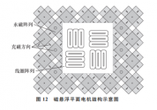
Tsinghua-U-Precision motors for the MagLev Wafer Stage.
It's important to note that the engineering work would have already been completed before the paper was written.Date received: 2022-04-13
- Status
- Not open for further replies.


