Chinese semiconductor industry

Status
Not open for further replies.

gelgoog

Lieutenant General
Registered Member
This is why we keep saying that Bloomberg is a garbage source and should be banned here .
Yeah. You are better off reading the news agencies Reuters, Associated Press, and the like than what passes for journalism on those rags. At least the news agencies still try to be impartial. The regular news stopped doing that like 20 years ago. Went back full hog to yellow journalism.

I think in the long run the semiconductor tools manufacture will move to China in a big way. It is the largest consumer market, and its semiconductor industries keep growing at a rapid pace. The reason ASML exists in a place like the Netherlands is a historic accident. Philips, from the Netherlands, used to be a major consumer electronics manufacturer in Europe. And ASML was designed to service them. Philips was one of the original investors in TSMC. So ASML machines were in TSMC. And TSMC grew to be the largest foundry in the world. Philips in the meantime basically dropped out of the consumer electronics market. Its electronics business was spun out as NXP. Now Philips make lightbulbs and medical equipment. And maybe not even lightbulbs that soon.
 
Last edited:

PopularScience

Junior Member
Registered Member
He has also said the one testing with ICRD is for 65nm resolution and that one is still waiting for mass production. So unless there is additional info, I'm going to assume the mass produced one is the same one that was declared as such by Shanghai gov't last year, which is most likely SSA600.

Havok said this. Dry machine is similar to Immersion machine. Most likely it is SSA800.
Please, Log in or Register to view URLs content!


作者
Please, Log in or Register to view URLs content!

别的设备材料先不论,仅光刻机要让他在产线稳定量产一般就需要几年,当然因为上微90nm干式机已量产,浸没机与干式机在结构上无太大改动所以验证时间会相对快一些。
 

tphuang

Lieutenant General
Staff member
Super Moderator
VIP Professional
Registered Member
006DKHfbgy1ha158k1p6xj30o5140go2.jpg
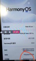
Not sure if everyone saw this today. They tested a Kirin chip on Mate 50. Here is what the Weibo Huawei whisper said.
今天相信大家都看到了这张图吧

工程机测试芯片,不要去想着会量产哈,这不可能的

我去年就说过,海思芯片团队不会放弃设计,必要的试片也是有可能的,制裁只是说不允许华为获得代工生产的资格。

所以设计会延续,不会因为不能生产就放弃迭代设计。不过高端麒麟真的暂时不要去想了,真的短期回不来的,也希望大家理解吧,产业链是一个整体,华为自己也无法突破,这需要整个中国一起努力,不过相信我们一定会突破的
so yes, they can keep designing and testing out more advanced chips, but it just can't get produced anytime soon. I don't know what he considers short term and whether or not they are waiting for full China production line here. But if SMIC can produce 5-7nm process smartphone chiplets in 2025, I don't see why they can't put it on medium level phone.
 

tokenanalyst

Brigadier
Registered Member
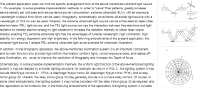
The Huawei EUV patent has some interesting details and one of which that is how they are going to power this machine. The are talking about using a EUV FEL.
1673582943804.png
The only way to get such powerful light source at least for the usage that they are planning is by using basically an accelerator. Like SSMB
1673583044905.png
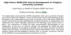
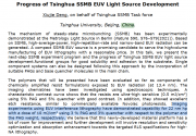
IDK the guys on Tsinhua said manage to pattern using EUV interference lithography some photo-resist using SSMB.

1673583790011.png1673583923042.png
Looks like Huawei is NOT even planning to compete with ASML,not even by a long shot, but they are looking for a tool that allows them to pattern the most critical layers of their chips.
 

PopularScience

Junior Member
Registered Member
The Huawei EUV patent has some interesting details and one of which that is how they are going to power this machine. The are talking about using a EUV FEL.
View attachment 104980
The only way to get such powerful light source at least for the usage that they are planning is by using basically an accelerator. Like SSMB
View attachment 104982
IDK the guys on Tsinhua said manage to pattern using EUV interference lithography some photo-resist using SSMB.

View attachment 104983View attachment 104984
Looks like Huawei is NOT even planning to compete with ASML,not even by a long shot, but they are looking for a tool that allows them to pattern the most critical layers of their chips.
This reminds me of Shenzhen FEL that will be completed in 2025
 

ansy1968

Brigadier
Registered Member
The Huawei EUV patent has some interesting details and one of which that is how they are going to power this machine. The are talking about using a EUV FEL.
View attachment 104980
The only way to get such powerful light source at least for the usage that they are planning is by using basically an accelerator. Like SSMB
View attachment 104982
IDK the guys on Tsinhua said manage to pattern using EUV interference lithography some photo-resist using SSMB.

View attachment 104983View attachment 104984
Looks like Huawei is NOT even planning to compete with ASML,not even by a long shot, but they are looking for a tool that allows them to pattern the most critical layers of their chips.
@tokenanalyst , @PopularScience Bro two competing or parallel development one in Beijing and other one in Shenzhen?
 
Status
Not open for further replies.
Top