Chinese semiconductor industry

Status
Not open for further replies.

tphuang

Lieutenant General
Staff member
Super Moderator
VIP Professional
Registered Member
Bro from my understanding it can't cause IF it does then Huawei will launch its topline smartphone. I'm no expert BUT the excerpt from our esteem members 14nm 3D chiplet is comparable in performance to TSMC 7nm therefore good enough for Huawei midfield phone.
Keep in mind that while you might be able to get the same computational power from stacking chiplets, it would still have worse power consumption. IIRC, power consumption is really a lot about the distance electricity have to travel between transistors. On a 14nm chiplet, there is just greater distance. But Huawei can compensate that on its phones by having more battery and better charging and such. Not going to match iPhone, but this is meant for lower end phones.

So, I saw trying to think why they are using 12nm chips here and I think it's a combination of N+1 tech not being matured enough and having limited capacity.

It looks like Huawei Mate 50 sold at least 10 million copies, so they'd probably put a lower end model to sell 25 million copies, which would require 50 million chiplets of 12/14 nm.

A simple math of 100 mm^2 (maybe smaller) chiplet would mean you can have maybe 500 good chips per wafer (assuming SMIC has solid yield on its 12/14nm process now). 50 million / 500 = 100k wafers or > 8k wafers a month. That's a lot of capacity out of the 35k wpm that SN1 can generate.

There is no way SMIC can dedicate that much of its N+1 production to 1 smartphone CPU client even if it's Huawei.

N+1 capacity right now is likely conserved for desktop/server CPU shops like Phytium and Hygon or even GPU makers (Moore threads maybe?). Even Loongson made the decision to stay with 12nm process for 3A6000 rather than go with N+1 capacity. I bet the yield and complexity for what they are producing using N+1 process still has some room for improvement.

So, SMIC needs to actually start production at SN2 (again, who knows where they are here) in order for Huawei phones to use more advanced domestic process.
 

olalavn

Senior Member
Registered Member
Bro from my understanding it can't cause IF it does then Huawei will launch its topline smartphone. I'm no expert BUT the excerpt from our esteem members 14nm 3D chiplet is comparable in performance to TSMC 7nm therefore good enough for Huawei midfield phone.
don't speculate too much, 14/12nm it will help a lot for 5G chip, Kunpeng, quantum chip... quantum chip they need most not SOC... cloud operation and their Euler is working strongest move...
Kirin will be fully available in 2024-2025... it will use RISC-V chip architecture
 

tokenanalyst

Brigadier
Registered Member
I'd guess Chinese equipment still not in volume production for 28nm is

1. Ion implantation
1673106312108.png
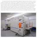
I saw the performance of Kingstone (wanye) Ion implanter is really closer to the competition Wanye is really close to SMIC, is very probably they already have deliver ion implanters for mass production.
CETC launched their 28nm Ion implanter in 2020, they claim good performance , my guess is already been use in mass production.

2. Wafer inspection and dimension measurement CD-SEM
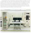
According DJEL the main producer of CD SEM and Ebeam defect detection their products already were delivered and verified by the costumers in 2021, early 2022, so is probably already use in mass production.
1673107241125.png1673107288851.png

Maybe someone with more insider information/knowledge can complete the list....
More than equipment, the bigger issues could be more:

-Materials, like producing enough quality photoresists and other high purity chemicals in enough quantity and quality. That could cause big bottlenecks.

-Mass producing these machines, even if Chinese tools are technically closer to US ones, can they produce enough of them? can they deliver them on time? LAM and AMAT have huge facilities to built this tools, Chinese companies like Naura and AMEC need to be more heavily subsidize so they can increase their production capacity and also pretty much every single critical tool company in the Chinese semiconductor industry. The good thing is that equipment manufacturing is more multi-disciplinary and is not like chip design that is more specific.

-Part and components, entice and verify companies closer to the semiconductor industry to start mass producing parts for semiconductor systems and subsystems manufacturers.

-The need of fully or close to fully domestic production lines to start solving bottlenecks, no just in equipment, but also all the support systems that allow those tools to work properly, like robots, managing software, chemical delivering systems, cleanroom systems, vacuum systems and sensing and so on. It doesn't matter if is only to produce chips for China state projects or for Huawei or if is just there to bleed money. This is something that should have been done years ago.
 

FairAndUnbiased

Brigadier
Registered Member
I'd guess Chinese equipment still not in volume production for 28nm is

1. Ion implantation

2. Wafer inspection and dimension measurement CD-SEM

Maybe someone with more insider information/knowledge can complete the list....
It's not just any individual tool. It's everything including how tools talk to each other, optimizing process flow, solving bottlenecks, domestication of components and components of components etc.
 

tokenanalyst

Brigadier
Registered Member
I heard stories about companies wanting to buy SMEE frontend machines, my guess is a least their I-line and/or KrF machines but their delivery times were simple just too long, so they just defaulted to ASML or Canon instead. It doesn't matter if the immersion lithography machine can process, as I heard, 200+WPH, has a MMO of 2.5nm and all the nice features. They have to make enough and deliver them on time. Production capacity in the Chinese supply chain is something that needs to be accelerated in 2023 and the coming years.​
 

tphuang

Lieutenant General
Staff member
Super Moderator
VIP Professional
Registered Member
I think what we want to stress is that the current project 02 development in china is just not ambitious enough. If you can only produce 20 arf dry and arfi scanners a year, that's just nowhere enough to satisfy the growing demand. Sure, it's unlikely the older arf scanners or krf or iline get sanctioned but china needs to invest more into fast tracking the production increase across it's supply chain. While this is not a process overnight, they really need to cut the bullshit and roll out a vision that actually meets the new geopolitical reality.
 

paiemon

Junior Member
Registered Member
I think what we want to stress is that the current project 02 development in china is just not ambitious enough. If you can only produce 20 arf dry and arfi scanners a year, that's just nowhere enough to satisfy the growing demand. Sure, it's unlikely the older arf scanners or krf or iline get sanctioned but china needs to invest more into fast tracking the production increase across it's supply chain. While this is not a process overnight, they really need to cut the bullshit and roll out a vision that actually meets the new geopolitical reality.
I would consider those two separate initiatives. Project 002 is an R&D endeavor coming up with an offering that is on par with prevailing international competitors and suitable for HVM. I think we are close to the finish line there. As for scaling up, that's more industrial policy, which may be more obscure as it would involve working with the supply chain and sub-system components. We just have to be patient, as external observers we only see the tip of the iceberg. For something as big, complex and involving as many systems as a DUVi scanner, an initial production run of 20 isn't too bad when you consider that it takes ASML about 3-6 months (if I am not mistaken) to put one together. I would also consider that its not just a components bottleneck holding back production increase, but also a labour force and training which probably takes just as long to get ready for something as sensitive as this.
 

tokenanalyst

Brigadier
Registered Member

Hechen New Materials completed a new round of financing of 100 million yuan, accelerating the domestic substitution of photomask substrates and CMP polishing materials​


image


Hechen New Materials has three categories of products: new display adsorption pads\polishing pads, photomask mask plate substrates, and CMP polishing materials for semiconductors, and has served more than 30 leading domestic customers.

Anhui Hechen New Materials Co., Ltd. (hereinafter referred to as "Hechen New Materials") completed a new round of financing of 100 million yuan, led by Shenzhen High-tech Investment, Anhui Jiangdong Industrial Investment, and Hexian Hesheng Investment , Chengdu Haisheng Junrong, Qingdao Huiwang and other institutions followed the investment, and the old shareholders Dongfang Fuhai and Hexian Fenghe Industry Guidance Fund continued to increase their investment. This round of financing will be mainly used to increase the production capacity of the existing Blank Mask 6-generation line and 8.5-generation Preparation for line expansion, and mass production of CMP polishing materials for semiconductors. Previously, the company had received tens of millions of financing led by Anhui Small and Medium Enterprise Development Fund.
image

Factory Photo
Hechen New Materials was established in 2016 and is located in Hexian Economic Development Zone, Maanshan City, Anhui Province. It mainly develops and produces new display/optical/semiconductor fine polishing materials and photomask substrates, focusing on domestic new display and semiconductor cards. A domestic alternative to neck material. Hechen New Materials has established a long-term and extensive cooperative relationship with the School of Polymer Science and Engineering of Sichuan University. It is a national high-tech enterprise and a "little giant" enterprise specialized in specialization and new technologies by the Ministry of Industry and Information Technology.For a long time, the main production consumables of the new display industry have relied on imports, and there is no substitute for similar products in China. After chip design companies design chip products, there are still restrictions and material shortage risks in the field of materials, and start-up companies in the field of materials have begun to attract industry attention.In September 2015, the company independently developed and successfully developed a new type of key consumable for display panel processing - adsorption pads. In October of the following year, the production line of adsorption pads was successfully put into production. According to Li Jiahai, this material fills the domestic gap and greatly reduces production costs.

Image


Absorbent pad

This is the first material product of Hechen New Materials. Since then, Hechen New Materials has begun to lay out other materials.So far, Hechen New Materials has three major categories of products: new display adsorption pads\polishing pads, photomask mask substrates, and CMP polishing materials for semiconductors. The company focuses on the domestic production of new display and semiconductor neck materials substitute.
.
Image


CMP polishing pad

According to Li Jiahai, in terms of adsorption pads, the company is at the leading level in the industry, breaking the long-term foreign monopoly; in the photomask substrate business, the company will continue to promote the 8.5th generation line photomask project while simultaneously expanding the production capacity of the 6th generation line It is expected to start trial production by the end of 2023 to achieve localized substitution; for CMP polishing materials, the company has passed multiple rounds of tests by domestic leading end customers, and has also conducted small-batch trial production in many domestic leading wafer companies. Small batch orders have been obtained, and mass production will be achieved in 2023.Li Jiahai told 36 Krypton: "In terms of product performance, Hechen New Materials can achieve the same level as foreign manufacturers or even better, with obvious price advantages, and realize domestic substitution. In addition, compared with foreign counterparts, it shortens the delivery cycle of downstream customers, Saves manufacturing costs."

Image


Please, Log in or Register to view URLs content!
 
Status
Not open for further replies.
Top