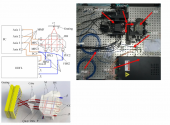
Russia has created a prototype of a lithography machine that can do 7nm.
"A lithographic installation is being developed at the Institute of Applied Physics of the Russian Academy of Sciences (IPF RAS) in Nizhny Novgorod. In 2011, a sample demonstrator of a lithograph with a working wavelength of 13.5 nm was built. It was a test stand in the framework of basic scientific research.
...
In 2018, scientists from the Institute of Physics and Technology of the Russian Academy of Sciences published a paper that presented experimental data on a laser-plasma X-ray source based on xenon.
The results obtained by our scientists in achieving an innovative method of nanolithography – massless X-ray lithography at a wavelength of 6.7 nm-were clearly demonstrated.
Instead of the molten tin source used in projection lithography by ASML, the Russian development uses a xenon-based target. With comparable efficiency, this significantly simplifies the source design and laser system, minimizes contamination of optical elements, reduces the operating wavelength by 20% when operating at a wavelength of 10.8 nm, and by 2 times - at a wavelength of 6.7 nm."
"But this is only one of the ways to develop Russian photolithography technology. There is another area of maskless EUV photolithography, namely the use of synchrotron radiation as the main source in lithographic equipment.
And in Russia, in March 2022, by order of the Ministry of Industry and Trade, they started developing the concept of a maskless X-ray photolithograph with a wavelength of less than 13.5 nm based on a synchrotron source. 670 million rubles were allocated for this work.
...
Photolithography based on synchrotron radiation should appear in 5-10 years.
...
It is noteworthy that synchrotron radiation is the next stage in the development of photolithography technology, thanks to which it is possible to achieve a transistor topology of less than 1 nm. But a particle accelerator should be attached to the factory.
Since the synchrotron can achieve stable radiation of even smaller wavelengths in the X-ray range, the technology will be the final evolution in lithographic equipment, where the produced nanostructures will be brought to the theoretical limit (less than 1 nm), when further reduction will be impossible.
Further technology will develop along the path of "layer cake" - transistors can only be placed one above the other."


