Chinese semiconductor industry

Status
Not open for further replies.

tokenanalyst

Brigadier
Registered Member

Cambrian: The company has completed the research and development of the fifth-generation intelligent processor micro-architecture and intelligent processor instruction set.​


1433192950729.8403664740937990.4059.png


Jiwei.com News On the evening of November 30, Cambrian released a summary of the latest investor research. The content of the minutes introduced the new progress of the company's intelligent processor micro-architecture and instruction set research and development, the company's cloud, edge product lines and corresponding application scenarios, and the progress of the company's vehicle chip research and development and productization.

It is reported that Cambrian has completed the research and development of the fifth-generation intelligent processor micro-architecture and intelligent processor instruction set. The fifth-generation intelligent processing architecture optimizes the storage hierarchy and improves the overall efficiency of the processor. On the basis of the advantages of the fourth generation, key optimizations have been carried out for emerging key application areas of intelligent algorithms, such as advertising recommendation systems, which can greatly improve the competitiveness of products in energy efficiency in related fields. The in-vehicle intelligent chip for high-end intelligent driving planned by the company will also adopt the Cambrian fifth-generation intelligent processor architecture and instruction set.

Cambricon's cloud product line currently includes cloud smart chips, accelerator cards, and training machines. Among them, cloud smart chips and accelerator cards are the basic units for artificial intelligence processing in cloud servers and data centers, which mainly provide energy-efficient hardware computing resources for artificial intelligence applications in cloud computing and data center scenarios. The company's training machine is provided by the company's self-developed cloud smart chip and accelerator card to provide computing power, and the whole machine is also self-developed by the company. The company's cloud products are currently mainly used in the Internet, finance and other fields.

Edge computing is equipped with moderate computing power on devices between small terminals and the cloud. Since it does not need to be uploaded to the cloud for processing, edge computing has lower latency, lower cost (such as saving network bandwidth) and more high reliability. The application scenarios of the Cambrian edge product market are more scattered than those of the cloud market. Edge products are mainly used in edge computing scenarios such as smart manufacturing, smart retail, smart education, smart home, and smart grid.

It is worth noting that Cambricon said about this year's target market expansion and revenue: "The company achieved operating income of 264 million yuan in the first three quarters of this year, and 92.5811 million yuan in single quarters in the third quarter, compared with the same period last year. Both have achieved steady growth to varying degrees, mainly due to the company’s increasingly rich array of cloud-end serialized products, the gradual improvement of product competitiveness, and the continuous optimization of the software ecosystem.”

Please, Log in or Register to view URLs content!
 

tokenanalyst

Brigadier
Registered Member
You referenced deceptive marketing message.

For any given node, there is a spectrum of easy to complex process steps. Just because a tool is used for one of plethora of process steps for a given node doesn't make it a "5nm etcher" that could handle all etch steps.

I can't reveal too much, but let me ask you, have you any clue which process step tsmc uses AMEC's etcher for? Do you really believe its for the most critical layer or process step?

Only Chinese WFE suppliers go out of their way to attach a process node designation to their equipment. They do this to create buzz to hype up their true capabilities. We don't typically do that in our industry. Only the process engineers, we know which model is good enough for which process step, application, node combination.

In our industry, tools are advertised more so by application and its performance spec. We don't typically use a "node" as an adjective/description for the equipment.
AMEC sells etching tools for dielectric materials, most their D series.
1669846088021.png

The sell plasma cleaning tools
1669846113081.png
They sell etching tools for NAND and DRAM
1669846292967.png

The have tools marketed for Oxide etching, like for hard mask and for Through Silicon Via Etching

1669846368813.png
As far I know TSMC does not do, NAND or DRAM and does not do packaging. And TSMC has been using AMEC for their 28nm process, but they have to verify a new etching tool for their 5nm process which lead me to believe is a new tool that was not in AMEC inventory at the time.

So they are either using the Primo AD for etching dielectric materials.
which I think is the material layer used to active the gates of the transistors. Sounds pretty critical to me.

1669844757915.png

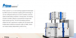
or the Primo Nanova for Oxide etching.
1669845572570.png

That is my guess
 

hvpc

Junior Member
Registered Member
So, are you saying non-SMIC customers mark up their chip prices so much more than SMIC customers that 5% global foundry revenue leads to end products only been like 1% global chip sales?

I have no idea how they measure these things, but there are a whole lot of new Chinese designed chips that are not actually made by Chinese fabs. do they only count chips that are designed and made by Chinese firms in that 6.6%?
No. IC Insight was comparing how much wafers in terms of revenue versus how much semiconductor consumed in China. The are saying, if all chips made by Chinese fabs (excluding foreign fabs like tsmc, Samsung, Hynix...) is consumed by China, this would only make up 6.6% of what China actually consumes.

You need to include Foundry, Memory, and other IDM as the baseline. Chinese foundries have about 10% total foundries revenue share, buy Chinese DRAM & 3DNAND revenue share are both <3%.

Let's do a quick estimate, China consumes 60% of semiconductor (sized at ~$550B in 2021), so we are looking at ~$330B demand. Domestic fab making up 6.6% of that would mean roughly $22B worth of wafers produced. Add up the Chinese foundry revenue (SMIC $6B = 5.5%....) so 10% total foundry share would mean $10B). CXMT & YMTC would add no more than $3B each (assuming 1.2M wafers each in 202). That leaves ~$6B chips by other IDM.

So IC Insight estimating Chinese fabs contributing $22B (6.6%) of overall China consumption of $330B seems about right.

BTW, don't hold me to exact numbers, I estimated these numbers off top of my head based on what I could remember. Numbers may not be exact, but I think I should have right number range/magnitude.

Essentially, IC Insight is also doing an estimation by estimating the Total Chinese semiconductor consumption and comparing it to an estimate of total wafer produced by domestic fab in terms of revenue. Now that I think about it, 340B & 23B comes to mind as familiar numbers.....so my quick analysis above of $330B/$22B are definitely close.
That's not what I'm saying at all.
I don't understand why they need to have same reliability, throughput and yield as their foreign counterpart? If there is no alternative to them, then Chinese fabs have to use them.
Without hitting an acceptable reliability, throughput, and yield would make fab operation a nightmare. Low reliability would take up too much resource; amount of time required to fix, requalify the tool, and effort to manage the WIP (work in progress) by moving wafers to a different equipment with different fingerprint is complex. If too many tool breaks down, too often, you'd end up with so many unique combination of tool-sets fingerpint to manage.

Low throughput means more equipment and fab space needed than baseline. Low yield not only impacts the bottom line (profit), but the extra work required to troubleshoot the yield issue would make a fab quite chaotic.

You just can't run a fab efficiently when basic reliability, yield, and throughput couldn't ne reached.

Anyhow, those comment about needing improvement on reliability, throughput, yield, is not mine. It's assessments I heard directly from domestic fabs. It's compilation & paraphrasing of what I heard...the few feedbacks I received are consistent that domestic tools meet a certain node in DRAM/3D-NAND/Logic, and they always come with the same comment on the "need improvement" areas.
From the Lam interview. They have very few employees serving at SMSC. It took 3 years for SMIC to find the tools to ramp up production at SN1 to probably 30k wpm. That's really slow. Seems like they were really hard pressed to get any American tools there.
A number I keep hearing is 20K wpm. Without divulging which company's tool is the bottleneck, the bottleneck at one of the process step (etch, deposition) must be at around 20K wpm.
SMIC said there were 2 things they were for. 1) ASML scanners 2) low production items that require long lead time. Which one do you think is taking bulk of the $1.6 billion Capex?
I agree the additional 1.6B is mostly going to the scanners. I just disagree they are for NXT2050/2100. SN1 doesn't need anymore scanners. SN2 will not take on tools until 2024 & without domestic equipment that could support 7nm, there won't be much need for NXT2050/2100. Even if SMIC do invest in 35K worth of 7nm, probably only need 2-3 NXT2050.
Let me ask you something. Huahong Capex for 2023 is like $1 billion (let's say 2022 is around the same) and it's adding probably 30k wpm 12-inch wafers next year. SMIC is maybe adding 50k wpm 12-inch wafers next year. It's Capex is $6.6 billion. How is SMIC spending 6 times as much Capex when its capacity expansion is just 60% more? It's basically spending 4x as much per wafer capacity added as Huahong. Is SMIC just throwing money around and wasting them? Huahong fab 7 was mostly adding 55-90 nm chips. Is 28 to 65 nm Capex supposed to be 4x of that? Seems unlikely based on the charts that everyone have been showcasing.


ASML said they delivered their first 2100i in Q3. Are you telling them there is a fab outside of China that needs 2100i? I'm not saying they bought that many NXT2050/2100i. Based on what others and ASML said, you don't need 2050/2100i outside of a few steps. I'm saying they've spent way more money per year on ASML scanners than they need to do if they were just adding 50k wpm of mature process capacity.
First, first few systems of a new model are essentially beta systems and need to be tested in production setting to help WFE supplier like ASML validate their new system. Under this limitation, you would already expect this first system to go to leading edge logic or DRAM fab.
And, 'yes', the new functionalities on NXT2100 are needed, mores o, outside of China. SMIC's N+2 nor any 7nm process in the world could bring out the new advanced capabilities of NXT2100.
Word on the street is the first NXT2100 was shipped to Japan. That's all I would/could reveal in this open forum.
We know for example, they spent $1.2 billion for the year before March 2021 on ASML scanners. We know they spend around $4.3 billion in Capex in both 2020 and 2021. Their original Capex plan was $5 billion for this year. So based on that, they were originally planning to spend around $1.5 billion in ASML scanners this year. Now since they added $1.6 billion to that for both early deposit and probably early deliveries. Let's say that will lead to $4.5 to 5 billion Capex with ASML in 2022/2023. Based on the cost of these machines. That seems way more than what they need for adding capacity at the new Beijing plant. They could be stocking up some machines or they could also be adding more capacity at SMSC fab.


I don't agree with that at all. I think their slow pace of expansion at SN1 after 2020 was due to not being able to get the American equipment they needed, hence they had to get less reliable/efficient domestic tools and take their time to ramp up with them.

And I think they've been really quiet about what they've been doing there, because it does them no good to talk about their advanced node achievement.


I think we can agree that they were not at 35k wpm for the entire year. I'd be surprised if they are at 35k wpm right now actually.
O-KAY!! Something we agree on! : D

Too many rebuttal from you to respond to, I just answered a few. I'll try to find time to respond to your other points
 

tonyget

Senior Member
Registered Member
I agree the additional 1.6B is mostly going to the scanners. I just disagree they are for NXT2050/2100. SN1 doesn't need anymore scanners. SN2 will not take on tools until 2024 & without domestic equipment that could support 7nm, there won't be much need for NXT2050/2100. Even if SMIC do invest in 35K worth of 7nm, probably only need 2-3 NXT2050.

Could it be SMIC's preemptive measure?Just in case they couldn't get it in the future,like what happened to their EUV purchases.
 
Last edited:

tokenanalyst

Brigadier
Registered Member
No. IC Insight was comparing how much wafers in terms of revenue versus how much semiconductor consumed in China. The are saying, if all chips made by Chinese fabs (excluding foreign fabs like tsmc, Samsung, Hynix...) is consumed by China, this would only make up 6.6% of what China actually consumes.

You need to include Foundry, Memory, and other IDM as the baseline. Chinese foundries have about 10% total foundries revenue share, buy Chinese DRAM & 3DNAND revenue share are both <3%.

Let's do a quick estimate, China consumes 60% of semiconductor (sized at ~$550B in 2021), so we are looking at ~$330B demand. Domestic fab making up 6.6% of that would mean roughly $22B worth of wafers produced. Add up the Chinese foundry revenue (SMIC $6B = 5.5%....) so 10% total foundry share would mean $10B). CXMT & YMTC would add no more than $3B each (assuming 1.2M wafers each in 202). That leaves ~$6B chips by other IDM.

So IC Insight estimating Chinese fabs contributing $22B (6.6%) of overall China consumption of $330B seems about right.

BTW, don't hold me to exact numbers, I estimated these numbers off top of my head based on what I could remember. Numbers may not be exact, but I think I should have right number range/magnitude.

Essentially, IC Insight is also doing an estimation by estimating the Total Chinese semiconductor consumption and comparing it to an estimate of total wafer produced by domestic fab in terms of revenue. Now that I think about it, 340B & 23B comes to mind as familiar numbers.....so my quick analysis above of $330B/$22B are definitely close.
A lot of those imported chips are chips used by foreign companies in their products and reexported back, some of those chips basically add to zero in China, because are not consumed domestically or used by domestic Chinese companies. Also we have to keep in mind that price is not volume. An Intel CPU may cost more than 100 microcontroller chips, measuring chips sales in dollars terms skew the analysis in favor of the most expensive chips. 70% in volume was always the goal of the goverment, the don't want to completely replace the domestic consumption, for now, of intel CPUs but chips like microcontrollers and power chips for example which in volume make the majority of the chips. Measured by volume is about close to 40%.
 

hvpc

Junior Member
Registered Member
Could it be SMIC's preemptive measure?Just in case they couldn't get it in the future,like what happened to their EUV purchases.
It's certainly preemptive measure. But not sure what the purpose it serves.

This was pre-payment or down payment for future scanner purchase. Any future US sanction on immersion scanners would certainly trump any down payment or an existing PO. SMIC had an outstanding EUV PO with ASML and also down payment, but they still weren't able to take delivery of the EUV system.

So not sure why it would be different this time around with the immersion systems. If US could coerce the Dutch government to block shipment of immersion scanner, even the $1.6B pre-payment will not guarantee SMIC could get ASML to honor the immersion POs.

I'm sure the $1.6B serves some purpose, I just personally don't quite understand what that purpose is.
 

hvpc

Junior Member
Registered Member
A lot of those imported chips are chips used by foreign companies in their products and reexported back, some of those chips basically add to zero in China, because are not consumed domestically or used by domestic Chinese companies. Also we have to keep in mind that price is not volume. An Intel CPU may cost more than 100 microcontroller chips, measuring chips sales in dollars terms skew the analysis in favor of the most expensive chips. 70% in volume was always the goal of the goverment, the don't want to completely replace the domestic consumption, for now, of intel CPUs but chips like microcontrollers and power chips for example which in volume make the majority of the chips. Measured by volume is about close to 40%.

Nominally, market share is based on revenue and not unit. If you look at typical semiconductor industry analysis, the market share is always based on revenue because revenue number are most readily available via financial reports, whereas exact number of chips require some assumptions and extrapolation.

The motivation of MIC2025 was based on the large trade deficit in semiconductors based on revenue. Even though MIC2025's 70% sefl-sufficiency target is a bit vague, it's widely accepted that it's based on revenue, at least by the semiconductor industry & by US government.

I highly doubt the Chinese government was aiming for 70% unit share by 2025. The emphasis was getting domestic fabs to invest in advanced nodes. If unit share was the target, we woudn't have seen so many fabs making 14nm and below as the target. It is this massive activity towards advanced, higher revenue chips that triggered the U.S.'s reaction. Furthermore, if 70% unit share is the true target, then 'radio silence' toward the west's interpretation of 70% revenue share screwed us over. I don't think the U.S. would've imposed the current sanction if they think China is after 70% unit share.

The cut-off point latest US sanction is also a clear indication the U.S. is not interested in expanding the likes of 28nm logic since it's not as profitable. U.S. is clearly going after, while depriving China access to, the higher revenue advanced nodes.
 

mst

Junior Member
Registered Member
"The best that SMIC's "Non-A" lines can produce at the moment is 40-nm chips, meaning the space between transistors is comparatively massive -- about half the size of a coronavirus particle. Such technology existed as far back as 2008. SMIC is trying to advance to 28-nm chips without relying on American equipment within two years, people with direct knowledge told Nikkei. SMIC did not respond to a request for comment."

This doesn't seem accurate to me?
 
Status
Not open for further replies.
Top