CXMT needs to develop higher density memory and DDR5. And AFAIK China still has no GDDR manufacture of its own. But it might be problematic to do so because of patents.
Also LPDDR5,which is main stream on today's smartphone
CXMT needs to develop higher density memory and DDR5. And AFAIK China still has no GDDR manufacture of its own. But it might be problematic to do so because of patents.
Maybe you are referring to this companyi think tokenanalyst posted related GDDR. one domestic firm is capable to produce. waiting for his response. coz i can't find the information as this thread has now over 2000 pages.
tokenanalyst
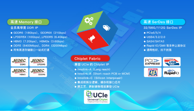
The domestic high-performance computing "three-piece" IP solution is released to meet the bandwidth requirements of the new generation of SoC
In the digital age, data storage, computing, transmission, and application requirements have become new driving forces. High-end chips such as cloud services and high-performance computing are inseparable from the support of underlying IP, especially DDR technology, Chiplet, and high-speed SerDes. Heavy. For high-computing SoC scenarios such as CPU/GPU/DPU/NPU commonly used in HPC, Innosilicon has launched a common IP platform centered on the " three-piece set " of high-performance computing.
The " three-piece set " of Innosilicon high-performance computing includes the world's top full-range high-end DDR series, the first Innolink™ Chiplet series compatible with UCIe standards, and the domestic leading SerDes (PCIe6/5) series, which can help customers optimize high- end Strict performance, power consumption, and cost targets on SoCs such as performance computing, AI, and graphics applications have greatly improved the efficiency of SoC R&D, reduced risks, and provided strong support for the upgrade of computing power requirements in the digital age.

▲ Industry-leading high-performance computing "three-piece" IP solution
The HPC IP "three-piece set" is the latest achievement of Innosilicon's 16 years of intensive cultivation of high-performance and high-reliability IP. It has three significant advantages: First, high-end performance. Regardless of DDR, Serdes or Chiplet, Innosilicon's performance is the world's leading , with the most complete interface coverage; the second is high-end process verification, high-end 10nm/8nm/7nm/6nm/5nm/3nm have been developed and verified and mass-produced by authorized customers; the third is cross-platform to ensure production safety, Innosilicon IP in TSMC /Samsung/GlobalFoundries/UMC/Intel/SMIC/Huali and other major foundries have all taped out and verified, and have authorized the mass production of billions of high-end SoC chips around the world, which can speed up SoC development and reduce risks.
The whole series of high-bandwidth DDR storage interface solutions break the memory wall
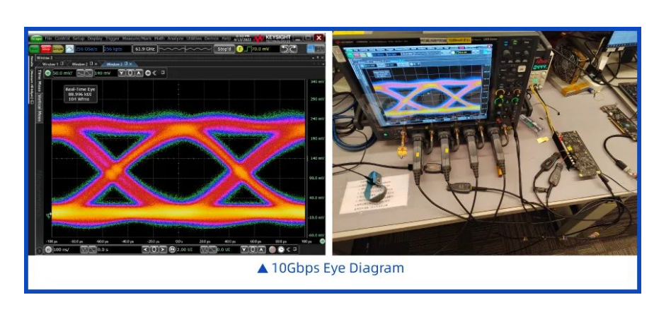
In terms of breaking through the memory wall technology, Innosilicon has the world's top full range of high-end DDR storage interface solutions. Not only took the lead in breaking through 10Gbps, mass-produced the world's fastest LPDDR5/5X Combo IP with advanced technology ; The rate is up to 7.2Gbps. All high-end DDR series IP can provide PHY and Controller overall solutions, and have been mass-produced and tested in advanced processes, fully support various JEDEC standards, in terms of performance and stability, size and power consumption, compatibility with more protocols, and application scenario optimization It is outstanding in terms of ease of use and integration, and can help breakthroughs in high-performance applications such as CPU/GPU/NPU high-performance computing, automotive autonomous driving, and mobile terminals.

▲The measured waveform of Innosilicon LPDDR5X (single-bit DQ up to 10Gbps) on a long-distance PCB board
Compatible with the UCIe Chiplet solution , breaking through the performance limit of a single chip
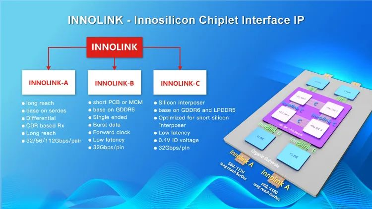
In response to the popular Chiplet technology, Innolink™ Chiplet, the first domestic cross-process and cross-package Chiplet connection solution-Innolink™ Chiplet, is the first to realize compatibility with two UCIe specifications (Innolink-B/C), helping chip design companies and system manufacturers to break through the single The limit of grain manufacturing and the performance bottleneck of a single chip have been successfully mass-produced on advanced technology. This solution not only supports standard packaging and advanced packaging, but also supports short-distance PCB scenarios. In various application scenarios, it has the advantages of low latency, low power consumption, high bandwidth density, and ultra-high cost performance. Covering D2D, C2C, B2B and other connection scenarios, it provides full-stack services such as packaging design, reliability verification, signal integrity analysis, DFT, thermal simulation, and test solutions.

▲Innolink™ Chiplet A/B/C implementation method
High-speed SerDes complete solution to open up the information highway
Innosilicon 32/56/64G SerDes complete solution has been at the international forefront in terms of speed, various interface standard types, silicon verification coverage and other important indicators, including PCIe6/5 (downward compatible with PCIe4/3/2), USB3.2/3.0, SATA, XAUI, SATA, RapidIO, CXL2.0, and the latest 112G SerDes are also under intensive development, with high compatibility, low cost, high performance, and high reliability, providing one-stop worry-free integration and flexible customization of Retimer Exchange chips with Switch for applications such as 5G communication, autonomous driving, artificial intelligence, big data storage, cloud computing, high-performance image media processing, and the Internet of Everything.
Right. Innosilicon does not make DDR5 wafers/chips.No. From what I understand Innosilicon make DDR5 memory controller IP blocks which you can add to your own chip design.
CXMT needs to develop higher density memory and DDR5. And AFAIK China still has no GDDR manufacture of its own. But it might be problematic to do so because of patents.
DDR5 grade DRAM chips are supported by D1z node DRAM. CXMT has just recently achieved D1x level capability.Also LPDDR5,which is main stream on today's smartphone
Not exactly. Not from a technical capability stand point.The good news is that the memory sector is at down turn cycle,major producers are cutting production,price dropped significantly. CXMT has few years time to wait domestic equipments to mature without worrying about expansion,hopefully by the time next memory upward cycle arrives,CXMT will be ready to expend with domestic equipments
No. SMIC accounts for 5% of foundry revenue NOT 5% of global chip sales.This can't be real. SMIC alone accounts for over 5% of global chip sales and they want to tell us that Chinese companies only account for 6.6% of their domestic market. That seems like complete nonsense.
You are correct. Currently, domestic WFE other than litho has been qualified only up to 28nm. Even then, these domestic equipment are still not at parity with industry's tools of record. We still have ways to go to improve domestic equipment's tool reliability, throughput, and yield.So, this non-A lines are just referring to its current Beijing fab that is not designed to produce any advanced chips and the new SMIC Capital JV that is also only doing 28nm+ process. So yes, I'm sure the best they can do is 28nm at these lines. The lines were never meant to do better than that!
SN1 expansion is basically completed. No more scanners needed and can't get access to American process equipment. Without American equipment, SN1 is unlikely to expand its wafer output; the bottleneck is limited by amount of American process equipment already purchased.Again, SMIC is being extremely secretive about its SN1/SN2 plans. It's acting like expansions here aren't even happening despite ramped up purchases of ASML scanners that are clearly geared for SMSC JV.
You think wrong, bud. Since SMIC could still buy ASML scanners, and you are aware and agree domestic non-litho equipment are at 28nm level.......American WFE is indeed the limiting factor for SMIC's SN1 & SN2.Recently, they changed the description of their business to 0.35微米到FinFET from 0.35 微米到 14 纳米. If they can't get all the ASML scanners they need, then their advanced node production will likely be slowed down. But I really don't think American tools are the limiting factor here. Will be interesting when we get the full years report and compare the revenue from SMSC JV vs the mid year report. If we see revenue more than double, then we know they are moving to more advanced nodes with higher production level.
There's quite a bit of equipment at 14 and and even lower though right? 28 is right where every equipment can hit yeah?No. SMIC accounts for 5% of foundry revenue NOT 5% of global chip sales.
You are correct. Currently, domestic WFE other than litho has been qualified only up to 28nm. Even then, these domestic equipment are still not at parity with industry's tools of record. We still have ways to go to improve domestic equipment's tool reliability, throughput, and yield.
SN1 expansion is basically completed. No more scanners needed and can't get access to American process equipment. Without American equipment, SN1 is unlikely to expand its wafer output; the bottleneck is limited by amount of American process equipment already purchased.
Your previous "predictions" on what SMIC's extra 1.6B CAPEX is for was not correct. Besides, like I said, the bottleneck at SN1 is not scanners. By the way, your prediction on NXT2050/2100 is too bullish. There aren't that many NXT2050 and there is no NXT2100 in China.
SN2 will not ramp for another year.
You think wrong, bud. Since SMIC could still buy ASML scanners, and you are aware and agree domestic non-litho equipment are at 28nm level.......American WFE is indeed the limiting factor for SMIC's SN1 & SN2.
With a full year of financial data, we will obviously see a great Y/Y revenue uptick. But, the revenue will definitely not reflect the full 35K wafer per month worth of revenue... Capacity in the beginning of the year is obviously lower than the second half of the year, so my guess we are more likely to see revenue reflecting 120K 14nm & 60K 7nm wafers for 2022.
Can you explain why domestic WFE is qualified only for 28 nm when there's reports TSMC has qualified AMEC etchers for 5 nm?No. SMIC accounts for 5% of foundry revenue NOT 5% of global chip sales.
You are correct. Currently, domestic WFE other than litho has been qualified only up to 28nm. Even then, these domestic equipment are still not at parity with industry's tools of record. We still have ways to go to improve domestic equipment's tool reliability, throughput, and yield.
SN1 expansion is basically completed. No more scanners needed and can't get access to American process equipment. Without American equipment, SN1 is unlikely to expand its wafer output; the bottleneck is limited by amount of American process equipment already purchased.
Your previous "predictions" on what SMIC's extra 1.6B CAPEX is for was not correct. Besides, like I said, the bottleneck at SN1 is not scanners. By the way, your prediction on NXT2050/2100 is too bullish. There aren't that many NXT2050 and there is no NXT2100 in China.
SN2 will not ramp for another year.
You think wrong, bud. Since SMIC could still buy ASML scanners, and you are aware and agree domestic non-litho equipment are at 28nm level.......American WFE is indeed the limiting factor for SMIC's SN1 & SN2.
With a full year of financial data, we will obviously see a great Y/Y revenue uptick. But, the revenue will definitely not reflect the full 35K wafer per month worth of revenue... Capacity in the beginning of the year is obviously lower than the second half of the year, so my guess we are more likely to see revenue reflecting 120K 14nm & 60K 7nm wafers for 2022.
You referenced deceptive marketing message.Can you explain why domestic WFE is qualified only for 28 nm when there's reports TSMC has qualified AMEC etchers for 5 nm?
