The domestic high-performance computing "three-piece" IP solution is released to meet the bandwidth requirements of the new generation of SoC
In the digital age, data storage, computing, transmission, and application requirements have become new driving forces. High-end chips such as cloud services and high-performance computing are inseparable from the support of underlying IP, especially DDR technology, Chiplet, and high-speed SerDes. Heavy.
For high-computing SoC scenarios such as CPU/GPU/DPU/NPU commonly used in HPC, Innosilicon has launched a common IP platform centered on the " three-piece set " of high-performance computing.
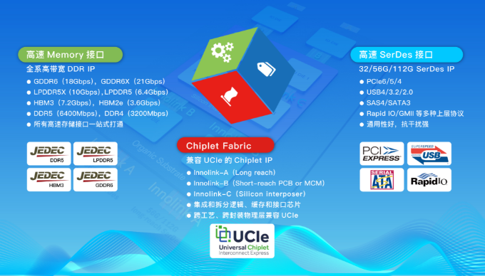
The " three-piece set " of Innosilicon high-performance computing includes the world's top full-range high-end DDR series, the first Innolink™ Chiplet series compatible with UCIe standards, and the domestic leading SerDes (PCIe6/5) series, which can help customers optimize high- end Strict performance, power consumption, and cost targets on SoCs such as performance computing, AI, and graphics applications have greatly improved the efficiency of SoC R&D, reduced risks, and provided strong support for the upgrade of computing power requirements in the digital age.
▲ Industry-leading high-performance computing "three-piece" IP solution
The HPC IP "three-piece set" is the latest achievement of Innosilicon's 16 years of intensive cultivation of high-performance and high-reliability IP. It has three significant advantages: First, high-end performance. Regardless of DDR, Serdes or Chiplet, Innosilicon's performance is the world's leading , with the most complete interface coverage; the second is high-end process verification, high-end 10nm/8nm/7nm/6nm/5nm/3nm have been developed and verified and mass-produced by authorized customers; the third is cross-platform to ensure production safety, Innosilicon IP in TSMC /Samsung/GlobalFoundries/UMC/Intel/SMIC/Huali and other major foundries have all taped out and verified, and have authorized the mass production of billions of high-end SoC chips around the world, which can speed up SoC development and reduce risks.
The whole series of high-bandwidth DDR storage interface solutions break the memory wall
In terms of breaking through the memory wall technology, Innosilicon has the world's top full range of high-end DDR storage interface solutions.
Not only took the lead in breaking through 10Gbps, mass-produced the world's fastest LPDDR5/5X Combo IP with advanced technology ; The rate is up to 7.2Gbps. All high-end DDR series IP can provide PHY and Controller overall solutions, and have been mass-produced and tested in advanced processes, fully support various JEDEC standards, in terms of performance and stability, size and power consumption, compatibility with more protocols, and application scenario optimization It is outstanding in terms of ease of use and integration, and can help breakthroughs in high-performance applications such as CPU/GPU/NPU high-performance computing, automotive autonomous driving, and mobile terminals.
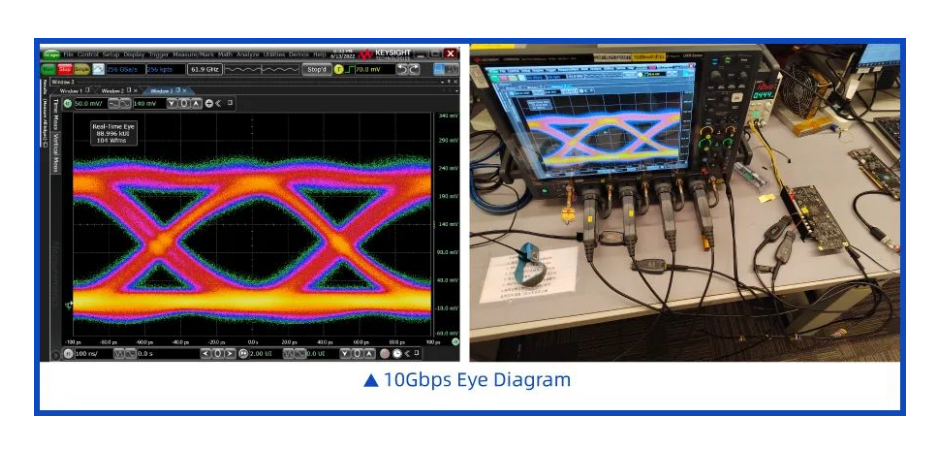
▲The measured waveform of Innosilicon LPDDR5X (single-bit DQ up to 10Gbps) on a long-distance PCB board
Compatible with the UCIe Chiplet solution , breaking through the performance limit of a single chip
In response to the popular Chiplet technology, Innolink™ Chiplet, the first domestic cross-process and cross-package Chiplet connection solution-Innolink™ Chiplet, is the first to realize compatibility with two UCIe specifications (Innolink-B/C), helping chip design companies and system manufacturers to break through the single The limit of grain manufacturing and the performance bottleneck of a single chip have been successfully mass-produced on advanced technology.
This solution not only supports standard packaging and advanced packaging, but also supports short-distance PCB scenarios. In various application scenarios, it has the advantages of low latency, low power consumption, high bandwidth density, and ultra-high cost performance. Covering D2D, C2C, B2B and other connection scenarios, it provides full-stack services such as packaging design, reliability verification, signal integrity analysis, DFT, thermal simulation, and test solutions.
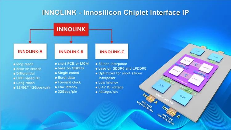
▲Innolink™ Chiplet A/B/C implementation method
High-speed SerDes complete solution to open up the information highway
Innosilicon 32/56/64G SerDes complete solution has been at the international forefront in terms of speed, various interface standard types, silicon verification coverage and other important indicators,
including PCIe6/5 (downward compatible with PCIe4/3/2), USB3.2/3.0, SATA, XAUI, SATA, RapidIO, CXL2.0, and the latest 112G SerDes are also under intensive development, with high compatibility, low cost, high performance, and high reliability, providing one-stop worry-free integration and flexible customization of Retimer Exchange chips with Switch for applications such as 5G communication, autonomous driving, artificial intelligence, big data storage, cloud computing, high-performance image media processing, and the Internet of Everything.


