Cadence和Synopsys特供中国版EDA工具曝光,中国市场仍举足轻重
集微网消息,受美国BIS于10月7日颁布的一系列针对中国的出口管制新规影响,可用于非平面晶体管架构(即FinFET或GAAFET)为16nm或14nm以下的逻辑芯片所必需的EDA软件,自10月14日起不能对中国客户出售,旨在打压中国在先进工艺上的发展脚步。
尽管针对GAAFET结构的EDA软件,是所有半导体公司进入3nm之后先进制程后都必须使用的工具,虽然不是当前国内IC设计公司的主流需求,但仍对产业信心造成了不小的打击。

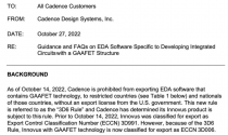
对于几大EDA龙头企业,显然也不想失去中国这个规模庞大的市场。根据集微网近日获取的一份邮件信息显示,Cadence已针对中国客户需求,推出特供国内客户使用的“出口版本”软件。
Innovus Implementation System为Cadence公司面向先进节点设计的设计实现平台,提供了数字后端(IC版图设计)所需的布局、优化、布线和时钟方面的功能。Innovus与Synopsys的ICC工具均为当前最主要的数字后端设计工具。
根据Cadence在10月27日发给客户的这份邮件,在10月14日新禁令生效之前,Innovus的出口控制分类编号被归类为 (ECCN)3D991,不限制向中国出售,但14日之后,受“3D6规则”限制,支持GAAFET技术的Innovus工具不能再向中国客户销售。
对此,Cadence推出了一个特供中国的InnovusExport21版本,删去了对GAAFET技术的支持和功能,而完整版则更名为Innovus211。
一位熟悉此事的设计人员向集微网透露,
国内客户在10月14日之前下载的完整版Innovus211仍然可以继续使用,但是之后最多也只能升级至22.3x版本;在14日之后国内(包括美国列出的其余受限国家)只能使用InnovusExport21版本,也能进行更新升级。“两个版本的软件从11月4日之后会使用各自的license key。”他表示。
此外,目前美国方面还不限制中国公司远程通过云服务使用Innovus211。也就是说,只要是服务器在非管制国家及地区的云服务商,目前还可以接入使用,但是这个漏洞估计很快也会被补上。“为此国内很多公司几周前已经疯狂下载了一波。”他表示。
据悉,Synopsys在11月11日也针对Fusion Compiler工具发布了类似的通知,分为完整版和出口版。资料显示,Fusion Compiler是业界唯一支持单一数据模型和黄金签核标准的RTL-to-GDSII产品。它采用可扩展性高的统一数据模型,并包含了业界黄金签核工具中的分析技术。它作为是新思科技Fusion Design Platform的核心,重新定义了逻辑合成、布局布线以及签核验证等传统EDA工具边界。
上述设计人员认为,估计三大EDA巨头都会进行类似的(版本切割)动作,以减少在华业务损失。
据集微网了解,目前国内涉及GAAFET工艺的设计公司,主要包括AI芯片、网络芯片、CPU/GPU/DPU、Arm CPU、矿机ASIC等,他们对5nm和更先进工艺有着切实的要求。
对于EDA公司而言,其盈利主要来自软件license的授权。在国内,EDA公司还根据出售的EDA工具的license个数进行收费,而且每个license通常是三年起售,不同的EDA工具单价差异非常大。由于数字后端布局布线工具的复杂度是最高,工作量也是在芯片设计当中是最大的,所以license单价是最贵的。
Cadence Innovus平台和Synopsys Fusion Compiler平台可以说都是非常重要的数字后端(物理设计)工具,需要和工艺结合紧密。
在国内众多EDA初创企业中,据集微网了解,在相应工具上有布局的公司包括立芯、鸿芯微纳和芯行纪,但是离真正应用到客户端还有不小的距离。
不久之前,英伟达针对禁令,也为中国客户推出了特供的A800,符合美国新的出口管制规定,可替代被新规限制出口的A100。
这是美国半导体公司首次公开,为遵循美国出口管制新规为中国制造先进处理器而做出的努力和成果。而此次曝光的Cadence和Synopsys的应对之举,均显示出中国在半导体市场上仍具有举足轻重的地位。
Cadence and Synopsys provide tailored version of EDA tools for China, the Chinese market still plays a decisive role
Affected by a series of new export control regulations against China promulgated by the US BIS on October 7, it can be used for EDA necessary for logic chips with non-planar transistor architectures (ie FinFET or GAAFET) of 16nm or below 14nm. Software, which cannot be sold to Chinese customers since October 14, aims to suppress China's development in advanced technology.
Although the EDA software for the GAAFET structure is a tool that all semiconductor companies must use after entering the advanced process after 3nm, although it is not the mainstream demand of domestic IC design companies, it still caused a big blow to industry confidence.
For several leading EDA companies, they obviously don't want to lose the huge market in China. According to an email message obtained by Jiwei.com recently, Cadence has launched an "export version" software specially for domestic customers to meet the needs of Chinese customers.
Innovus Implementation System is Cadence's design implementation platform for advanced node design, which provides the layout, optimization, routing and clocking functions required by the digital backend (IC layout design). The ICC tools of Innovus and Synopsys are currently the most important digital back-end design tools.
According to this email sent to customers by Cadence on October 27, before the new ban came into effect on October 14, Innovus’s export control classification number was classified as (ECCN) 3D991, which does not restrict sales to China, but after the 14th , restricted by the "3D6 rules", Innovus tools supporting GAAFET technology can no longer be sold to Chinese customers.
In this regard, Cadence launched a version of InnovusExport21 specially for China, which deleted the support and functions of GAAFET technology, and the full version was renamed Innovus211.
A designer familiar with the matter revealed to Jiwei.com that the full version of Innovus211 downloaded by domestic customers before October 14th can still be used, but after that, they can only upgrade to version 22.3x at most; after the 14th, domestic ( Including the remaining restricted countries listed in the United States) can only use the InnovusExport21 version, and can also be updated. "The two versions of the software will use their respective license keys after November 4th," he said.
In addition, the United States currently does not restrict Chinese companies from remotely using Innovus211 through cloud services. In other words, as long as the server is a cloud service provider in a non-regulated country and region, it can still be accessed and used at present, but this loophole is expected to be filled soon. "For this reason, many domestic companies have downloaded a wave of crazy a few weeks ago." He said.
It is reported that Synopsys also issued a similar notice for the Fusion Compiler tool on November 11, which is divided into a full version and an export version. According to the data, Fusion Compiler is the only RTL-to-GDSII product in the industry that supports a single data model and golden signoff standard. It uses a highly scalable unified data model and includes analytics from the industry's gold sign-off tools. As the core of Synopsys' Fusion Design Platform, it redefines the boundaries of traditional EDA tools such as logic synthesis, place and route, and signoff verification.
The above-mentioned designers believe that it is estimated that the three major EDA giants will carry out similar (version cutting) actions to reduce business losses in China.
According to Jiwei.com, currently domestic design companies involved in GAAFET technology mainly include AI chips, network chips, CPU/GPU/DPU, Arm CPU, mining machine ASIC, etc. They have practical requirements for 5nm and more advanced technology.
For EDA companies, their profits mainly come from the authorization of software licenses. In China, EDA companies also charge according to the number of licenses of EDA tools sold, and each license is usually sold for three years, and the unit price of different EDA tools varies greatly. Since the complexity of digital back-end layout and routing tools is the highest, and the workload is also the largest in chip design, the unit price of the license is the most expensive.
Both the Cadence Innovus platform and the Synopsys Fusion Compiler platform can be said to be very important digital back-end (physical design) tools, which need to be closely integrated with the process.
Among the many domestic EDA start-ups, according to Jiweiwang, the companies that have layout in the corresponding tools include Laxcen, Hongxinwei and Xinxingji, but there is still a long way to go before the actual application to the client.
Not long ago, in response to the ban, Nvidia also launched a special A800 for Chinese customers, which complies with the new US export control regulations and can replace the A100 that is restricted by the new regulations.
This is the first time that a U.S. semiconductor company has made public its efforts and achievements to manufacture advanced processors for China in compliance with the new U.S. export control regulations. The responses of Cadence and Synopsys exposed this time show that China still plays a decisive role in the semiconductor market.


