Chinese semiconductor industry

Status
Not open for further replies.

ansy1968

Brigadier
Registered Member
The kind of hubris and 'Russia brings nothing to the table' attitude I'm reading here is no different from the West's on China.
I totally agree with you bro, Russia had a lot to offer, maybe a joint effort with China is possible as the Russian are keen to develop a DUVL equivalent to ASML NXT 2000i, my prediction if they do it alone within 5 years they may able to produce a working prototype BUT JV with SMEE they can have the machine by next year. ;)

Russian University Vows to Build 7nm Chipmaking Tools​

By
Please, Log in or Register to view URLs content!

published about 5 hours ago
Russian institute plans to build 7nm-capable scanner that beats ASML's analogue in several years.
Please, Log in or Register to view URLs content!

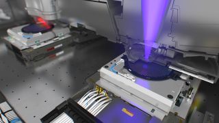
ASML EUV machine

(Image credit: ASML)

A Russian institute is developing its own lithography scanner that could produce chips using 7nm-class fabrication technologies. The machine is under development, with the plan to build it by 2028. When it is ready, it should be more efficient than ASML's Twinscan NXT:2000i tool, whose development took over a decade.

After Russia unleashed its bloody war against Ukraine on February 24, Taiwan was quick to ban shipments of advanced chips to the nation. The U.S., the U.K., and the E.U. then followed up with sanctions that effectively prohibit virtually all contract chipmakers with advanced fabs from working with Russian entities. In addition, companies like Arm cannot license their technologies to Russia-based chip designers. As a result, the Russian government rolled out a national program to develop the country's own 28nm-class fabrication technology by 2030, reverse engineer as many foreign chips as possible, and educate local talent to work on domestic chips.
However, there is a problem with a 28nm-class production node by 2030. Russia's most advanced fab can produce chips using a 65nm fabrication technology. Meanwhile, American and European makers of fab tools cannot supply their equipment to Russia due to sanctions, so the country has to design and build domestic wafer production equipment if it wants to adopt a 28nm node. Essentially, what has taken companies like ASML and Applied Materials decades to develop and iterate has to be done in about eight years.


Apparently, the Russian Institute of Applied Physics of the Russian Academy of Sciences intends to beat all expectations and produce a 7nm-capable lithography scanner by 2028, according to its plans published on
Please, Log in or Register to view URLs content!
website (via
Please, Log in or Register to view URLs content!
).
A modern lithography scanner capable of processing wafers using a 7nm-class process technology is a highly complex apparatus that involves a high-performance light source, sophisticated optics, and precise metrology, just to name a few critical parts. However, as a leading applied physics university in Russia, IAP believes that it can develop such a tool in a relatively short amount of time.

The tool will be somewhat different from scanners produced by companies like ASML or Nikon. For example, IAP plans to use a >600W light source (total power, not intermediate focus power) with an 11.3nm exposure wavelength (EUV wavelength is 13.5nm), which will require considerably more sophisticated optics than exists today. Because the light source of the device will be relatively low power, it will make the tool more compact and easier to build. Yet, it also means that its production of the scanner will be considerably lower than that of modern deep ultraviolet (DUV) tools. That might not be a problem, according to IAP.
When it comes to timing, IAP may be slightly too optimistic. For everything below 32nm, chipmakers use the so-called immersion lithography (which is essentially a booster to DUV tools). ASML
Please, Log in or Register to view URLs content!
its first immersion lithography system — the Twinscan XT:1250i — in late 2003 with a plan to deliver one in Q3 2004 to produce 65nm logic chips and 70nm half-pitch DRAMs. It took the company about five years and another generation of tools to
Please, Log in or Register to view URLs content!
its 32nm-capable Twinscan NXT:1950i in late 2008, with customer deliveries starting in 2009.
Then, it took the market leader some nine years to deliver its 7nm and 5nm-capable
Please, Log in or Register to view URLs content!
tool in 2018. TSMC used less advanced tools with multi-patterning for its first-generation N7 fabrication technology, but the timing of ASML’s introductions demonstrate how hard it is to transition from 65nm to 7nm. It took ASML 14 years to go from 65nm to 7nm. Now, IAP, which does not have any experience in chip production or ties with chipmakers, intends to build a 7nm-capable machine for volume production from scratch in about six years. While the plan does not sound feasible, it looks like IAP is full of enthusiasm.
"ASML, the global lithography leader, has been developing its EUV lithography system for almost 20 years and the technology has turned out to be incredibly complex," said Nikolai Chkhalo, Deputy Director of the Institute of Physics of Microstructures of the Russian Academy of Sciences for scientific and technological development. "The main objective of ASML in this case was to maintain the extremely high productivity that is needed only at the world's largest factories. In Russia, no one needs such high productivity. In our work, we start from the needs and tasks faced by domestic microelectronics — and this is not so much about quantity, but about quality. First of all, we need to transit to our own fabrication processes, develop our own design standards, our own tools, engineering, materials, so our own path is inevitable here. In fact, we need to balance between simplicity and performance."
IAP plans to build a fully functional alpha scanner by 2024. This one will not have to offer high productivity or maximum resolution but will have to work and be attractive to potential investors. IAP intends to build a beta version of the scanner with higher productivity and resolution by 2026. This machine should be mass production ready, but its productivity is not expected to be at its maximum. The final iteration of the litho scanner is said to emerge in 2028. It should get a high-performance light source (hence better productivity), better metrology and overall capabilities. There is no word how many of such machines IAP and/or its production partners will be able to produce by 2028.
It should be noted that fab equipment is not limited to lithography scanners. There are other types of machines performing etching, deposition, resist removal, metrology, and inspection operations that are not made in Russia. Furthermore, there is somewhat less advanced machinery like ultrapure air and water generators which also are not produced in Russia. Even if IAP RAS manages to build a lithography tool, Russia will still be a few hundred tools short of building a modern fab. Also, fabs need ultrapure raw materials produced in countries that will not supply to Russia.
 
Last edited:

weig2000

Captain
I totally agree with you bro, Russia had a lot to offer, maybe a joint effort with China is possible as the Russian are keen to develop a DUVL equivalent to ASML NXT 2000i, my prediction if they do it alone within 5 years they may able to produce a working prototype BUT JV with SMEE they can have the machine by next year. ;)

Russian University Vows to Build 7nm Chipmaking Tools​

By
Please, Log in or Register to view URLs content!

published about 5 hours ago
Russian institute plans to build 7nm-capable scanner that beats ASML's analogue in several years.

Please, Log in or Register to view URLs content!

ASML EUV machine

(Image credit: ASML)

A Russian institute is developing its own lithography scanner that could produce chips using 7nm-class fabrication technologies. The machine is under development, with the plan to build it by 2028. When it is ready, it should be more efficient than ASML's Twinscan NXT:2000i tool, whose development took over a decade.

After Russia unleashed its bloody war against Ukraine on February 24, Taiwan was quick to ban shipments of advanced chips to the nation. The U.S., the U.K., and the E.U. then followed up with sanctions that effectively prohibit virtually all contract chipmakers with advanced fabs from working with Russian entities. In addition, companies like Arm cannot license their technologies to Russia-based chip designers. As a result, the Russian government rolled out a national program to develop the country's own 28nm-class fabrication technology by 2030, reverse engineer as many foreign chips as possible, and educate local talent to work on domestic chips.
However, there is a problem with a 28nm-class production node by 2030. Russia's most advanced fab can produce chips using a 65nm fabrication technology. Meanwhile, American and European makers of fab tools cannot supply their equipment to Russia due to sanctions, so the country has to design and build domestic wafer production equipment if it wants to adopt a 28nm node. Essentially, what has taken companies like ASML and Applied Materials decades to develop and iterate has to be done in about eight years.


Apparently, the Russian Institute of Applied Physics of the Russian Academy of Sciences intends to beat all expectations and produce a 7nm-capable lithography scanner by 2028, according to its plans published on
Please, Log in or Register to view URLs content!
website (via
Please, Log in or Register to view URLs content!
).
A modern lithography scanner capable of processing wafers using a 7nm-class process technology is a highly complex apparatus that involves a high-performance light source, sophisticated optics, and precise metrology, just to name a few critical parts. However, as a leading applied physics university in Russia, IAP believes that it can develop such a tool in a relatively short amount of time.

The tool will be somewhat different from scanners produced by companies like ASML or Nikon. For example, IAP plans to use a >600W light source (total power, not intermediate focus power) with an 11.3nm exposure wavelength (EUV wavelength is 13.5nm), which will require considerably more sophisticated optics than exists today. Because the light source of the device will be relatively low power, it will make the tool more compact and easier to build. Yet, it also means that its production of the scanner will be considerably lower than that of modern deep ultraviolet (DUV) tools. That might not be a problem, according to IAP.
When it comes to timing, IAP may be slightly too optimistic. For everything below 32nm, chipmakers use the so-called immersion lithography (which is essentially a booster to DUV tools). ASML
Please, Log in or Register to view URLs content!
its first immersion lithography system — the Twinscan XT:1250i — in late 2003 with a plan to deliver one in Q3 2004 to produce 65nm logic chips and 70nm half-pitch DRAMs. It took the company about five years and another generation of tools to
Please, Log in or Register to view URLs content!
its 32nm-capable Twinscan NXT:1950i in late 2008, with customer deliveries starting in 2009.
Then, it took the market leader some nine years to deliver its 7nm and 5nm-capable
Please, Log in or Register to view URLs content!
tool in 2018. TSMC used less advanced tools with multi-patterning for its first-generation N7 fabrication technology, but the timing of ASML’s introductions demonstrate how hard it is to transition from 65nm to 7nm. It took ASML 14 years to go from 65nm to 7nm. Now, IAP, which does not have any experience in chip production or ties with chipmakers, intends to build a 7nm-capable machine for volume production from scratch in about six years. While the plan does not sound feasible, it looks like IAP is full of enthusiasm.
"ASML, the global lithography leader, has been developing its EUV lithography system for almost 20 years and the technology has turned out to be incredibly complex," said Nikolai Chkhalo, Deputy Director of the Institute of Physics of Microstructures of the Russian Academy of Sciences for scientific and technological development. "The main objective of ASML in this case was to maintain the extremely high productivity that is needed only at the world's largest factories. In Russia, no one needs such high productivity. In our work, we start from the needs and tasks faced by domestic microelectronics — and this is not so much about quantity, but about quality. First of all, we need to transit to our own fabrication processes, develop our own design standards, our own tools, engineering, materials, so our own path is inevitable here. In fact, we need to balance between simplicity and performance."
IAP plans to build a fully functional alpha scanner by 2024. This one will not have to offer high productivity or maximum resolution but will have to work and be attractive to potential investors. IAP intends to build a beta version of the scanner with higher productivity and resolution by 2026. This machine should be mass production ready, but its productivity is not expected to be at its maximum. The final iteration of the litho scanner is said to emerge in 2028. It should get a high-performance light source (hence better productivity), better metrology and overall capabilities. There is no word how many of such machines IAP and/or its production partners will be able to produce by 2028.
It should be noted that fab equipment is not limited to lithography scanners. There are other types of machines performing etching, deposition, resist removal, metrology, and inspection operations that are not made in Russia. Furthermore, there is somewhat less advanced machinery like ultrapure air and water generators which also are not produced in Russia. Even if IAP RAS manages to build a lithography tool, Russia will still be a few hundred tools short of building a modern fab. Also, fabs need ultrapure raw materials produced in countries that will not supply to Russia.

I was really impressed by the enthusiasm and confidence expressed by these Russian scientists from IAP, particularly considering Russia's best process node is at 90nm and they have been struggling to fab at 65nm for many years now, using imported equipment.

Until the last paragraph, that is, which really pours a lot of cold water on the idea.
 

ansy1968

Brigadier
Registered Member
I was really impressed by the enthusiasm and confidence expressed by these Russian scientists from IAP, particularly considering Russia's best process node is at 90nm and they have been struggling to fab at 65nm for many years now, using imported equipment.

Until the last paragraph, that is, which really pours a lot of cold water on the idea.
Bro can you see a collaboration? I know the Chinese are busy ramping up the production of SMEE SSA800 DUVL and vetting local vendors suppliers as urgency dictates with US adversarial attitude, so it may force the Russian to do it alone cause I'm thinking by that timeframe SMEE/CETC may have mass produce a machine equivalent to NXT 2100i , so why not buy it instead?
 

FairAndUnbiased

Brigadier
Registered Member
I was really impressed by the enthusiasm and confidence expressed by these Russian scientists from IAP, particularly considering Russia's best process node is at 90nm and they have been struggling to fab at 65nm for many years now, using imported equipment.

Until the last paragraph, that is, which really pours a lot of cold water on the idea.
The last paragraph just means that Chinese equipment strengths in deposition, etch, clean, etc. will compliment the lithography effort by Russia. I also think that they're OK because they don't have the ambition of high throughput, which is much harder than something that just works.
 

Weaasel

Senior Member
Registered Member
I totally agree with you bro, Russia had a lot to offer, maybe a joint effort with China is possible as the Russian are keen to develop a DUVL equivalent to ASML NXT 2000i, my prediction if they do it alone within 5 years they may able to produce a working prototype BUT JV with SMEE they can have the machine by next year. ;)

Russian University Vows to Build 7nm Chipmaking Tools​

By
Please, Log in or Register to view URLs content!

published about 5 hours ago
Russian institute plans to build 7nm-capable scanner that beats ASML's analogue in several years.

Please, Log in or Register to view URLs content!

ASML EUV machine

(Image credit: ASML)

A Russian institute is developing its own lithography scanner that could produce chips using 7nm-class fabrication technologies. The machine is under development, with the plan to build it by 2028. When it is ready, it should be more efficient than ASML's Twinscan NXT:2000i tool, whose development took over a decade.

After Russia unleashed its bloody war against Ukraine on February 24, Taiwan was quick to ban shipments of advanced chips to the nation. The U.S., the U.K., and the E.U. then followed up with sanctions that effectively prohibit virtually all contract chipmakers with advanced fabs from working with Russian entities. In addition, companies like Arm cannot license their technologies to Russia-based chip designers. As a result, the Russian government rolled out a national program to develop the country's own 28nm-class fabrication technology by 2030, reverse engineer as many foreign chips as possible, and educate local talent to work on domestic chips.
However, there is a problem with a 28nm-class production node by 2030. Russia's most advanced fab can produce chips using a 65nm fabrication technology. Meanwhile, American and European makers of fab tools cannot supply their equipment to Russia due to sanctions, so the country has to design and build domestic wafer production equipment if it wants to adopt a 28nm node. Essentially, what has taken companies like ASML and Applied Materials decades to develop and iterate has to be done in about eight years.


Apparently, the Russian Institute of Applied Physics of the Russian Academy of Sciences intends to beat all expectations and produce a 7nm-capable lithography scanner by 2028, according to its plans published on
Please, Log in or Register to view URLs content!
website (via
Please, Log in or Register to view URLs content!
).
A modern lithography scanner capable of processing wafers using a 7nm-class process technology is a highly complex apparatus that involves a high-performance light source, sophisticated optics, and precise metrology, just to name a few critical parts. However, as a leading applied physics university in Russia, IAP believes that it can develop such a tool in a relatively short amount of time.

The tool will be somewhat different from scanners produced by companies like ASML or Nikon. For example, IAP plans to use a >600W light source (total power, not intermediate focus power) with an 11.3nm exposure wavelength (EUV wavelength is 13.5nm), which will require considerably more sophisticated optics than exists today. Because the light source of the device will be relatively low power, it will make the tool more compact and easier to build. Yet, it also means that its production of the scanner will be considerably lower than that of modern deep ultraviolet (DUV) tools. That might not be a problem, according to IAP.
When it comes to timing, IAP may be slightly too optimistic. For everything below 32nm, chipmakers use the so-called immersion lithography (which is essentially a booster to DUV tools). ASML
Please, Log in or Register to view URLs content!
its first immersion lithography system — the Twinscan XT:1250i — in late 2003 with a plan to deliver one in Q3 2004 to produce 65nm logic chips and 70nm half-pitch DRAMs. It took the company about five years and another generation of tools to
Please, Log in or Register to view URLs content!
its 32nm-capable Twinscan NXT:1950i in late 2008, with customer deliveries starting in 2009.
Then, it took the market leader some nine years to deliver its 7nm and 5nm-capable
Please, Log in or Register to view URLs content!
tool in 2018. TSMC used less advanced tools with multi-patterning for its first-generation N7 fabrication technology, but the timing of ASML’s introductions demonstrate how hard it is to transition from 65nm to 7nm. It took ASML 14 years to go from 65nm to 7nm. Now, IAP, which does not have any experience in chip production or ties with chipmakers, intends to build a 7nm-capable machine for volume production from scratch in about six years. While the plan does not sound feasible, it looks like IAP is full of enthusiasm.
"ASML, the global lithography leader, has been developing its EUV lithography system for almost 20 years and the technology has turned out to be incredibly complex," said Nikolai Chkhalo, Deputy Director of the Institute of Physics of Microstructures of the Russian Academy of Sciences for scientific and technological development. "The main objective of ASML in this case was to maintain the extremely high productivity that is needed only at the world's largest factories. In Russia, no one needs such high productivity. In our work, we start from the needs and tasks faced by domestic microelectronics — and this is not so much about quantity, but about quality. First of all, we need to transit to our own fabrication processes, develop our own design standards, our own tools, engineering, materials, so our own path is inevitable here. In fact, we need to balance between simplicity and performance."
IAP plans to build a fully functional alpha scanner by 2024. This one will not have to offer high productivity or maximum resolution but will have to work and be attractive to potential investors. IAP intends to build a beta version of the scanner with higher productivity and resolution by 2026. This machine should be mass production ready, but its productivity is not expected to be at its maximum. The final iteration of the litho scanner is said to emerge in 2028. It should get a high-performance light source (hence better productivity), better metrology and overall capabilities. There is no word how many of such machines IAP and/or its production partners will be able to produce by 2028.
It should be noted that fab equipment is not limited to lithography scanners. There are other types of machines performing etching, deposition, resist removal, metrology, and inspection operations that are not made in Russia. Furthermore, there is somewhat less advanced machinery like ultrapure air and water generators which also are not produced in Russia. Even if IAP RAS manages to build a lithography tool, Russia will still be a few hundred tools short of building a modern fab. Also, fabs need ultrapure raw materials produced in countries that will not supply to Russia.
The last paragraph...

"There are other types of machines performing etching, deposition, resist removal, metrology, and inspection operations that are not made in Russia. Furthermore, there is somewhat less advanced machinery like ultrapure air and water generators which also are not produced in Russia. Even if IAP RAS manages to build a lithography tool, Russia will still be a few hundred tools short of building a modern fab. Also, fabs need ultrapure raw materials produced in countries that will not supply to Russia."

Two things, even if it is indeed the case that Russia doesn't have Russian made equipment that undertake all these operations at any level, which I am sceptical about:

- Russia can concurrently develop such equipment just as it develops lithographic equipment.
- China does produce all the equipment and materials mentioned - free of American and other foreign inputs - at decent to high quality and it can sell them to Russia.
 

FairAndUnbiased

Brigadier
Registered Member
The last paragraph...

"There are other types of machines performing etching, deposition, resist removal, metrology, and inspection operations that are not made in Russia. Furthermore, there is somewhat less advanced machinery like ultrapure air and water generators which also are not produced in Russia. Even if IAP RAS manages to build a lithography tool, Russia will still be a few hundred tools short of building a modern fab. Also, fabs need ultrapure raw materials produced in countries that will not supply to Russia."

Two things, even if it is indeed the case that Russia doesn't have Russian made equipment that undertake all these operations at any level, which I am sceptical about:

- Russia can concurrently develop such equipment just as it develops lithographic equipment.
- China does produce all the equipment and materials mentioned - free of American and other foreign inputs - at decent to high quality and it can sell them to Russia.
China can produce all the equipment around lithography such as clean/etch/deposition/develop/metrology, its just lithography that China has a problem with. This is not surprising to me in the least. If you follow the thread you'll see tons of links and reports from companies like AMEC, Naura, ACM, etc (etch/dep/clean), but one general rule I find works well: China has problems with mechanical engineering but is strong in electronics and chemistry. Etch/deposition/clean/develop is all chemistry, metrology is all electronics. Meanwhile a general rule is Russia has problems with electronics hardware but has strengths in mechanical engineering and software. lithography is heavily dependent on mechanical engineering for key components like wafer stage and mask management, and software for controls. I would not be surprise by significant Russian progress on their lithography instrument, and I would not be surprised by China helping Russia build the ecosystem around it.
 

mmbro

New Member
Registered Member
Current semicon situation in China reminiscing the development of nuclear weapons in China.
Unfortunately, Rubio & co do not read history books.

'Stillman said Chinese physicists told him that they had begun research on miniaturization during the 1970s, but could not complete it because they lacked the computing power to carry out massive calculations. When the Chinese physicists got access to supercomputers [[my note: that is, China's own supercomputer, developed in China by late 1980s]], they pulled out their old research, ran the numbers and designed the new devices.

On a visit to China in the summer of 1999, Stillman said, Hu Side, one of China's leading weapons physicists, delivered an angry speech over dinner about distortions he ascribed to the Cox committee and the prosecution of Taiwanese American scientist Wen Ho Lee for security violations.

As for miniaturization, "We did not need you," Hu Side said, according to Stillman. "These allegations must have been made for political reasons."

Please, Log in or Register to view URLs content!
 

tokenanalyst

Brigadier
Registered Member
China can produce all the equipment around lithography such as clean/etch/deposition/develop/metrology, its just lithography that China has a problem with. This is not surprising to me in the least. If you follow the thread you'll see tons of links and reports from companies like AMEC, Naura, ACM, etc (etch/dep/clean), but one general rule I find works well: China has problems with mechanical engineering but is strong in electronics and chemistry. Etch/deposition/clean/develop is all chemistry, metrology is all electronics. Meanwhile a general rule is Russia has problems with electronics hardware but has strengths in mechanical engineering and software. lithography is heavily dependent on mechanical engineering for key components like wafer stage and mask management, and software for controls. I would not be surprise by significant Russian progress on their lithography instrument, and I would not be surprised by China helping Russia build the ecosystem around it.
Well is not just mechanics but precision mechanics or better yet, is mechatronics, precision robotics, given that fact that the Russians built jet engines lead me to believe that the Russians don't lack in that area. But as far as I know only two nations have been able to built a high speed dual wafer stage with nanometer level of accuracy and controlled by highly complex motion algorithms: The Netherlands and China.
And as far I know only three can do high speed single wafer stage with nanometer lever accuracy: Japan, the Netherlands and China.

1666429359286.png

Please, Log in or Register to view URLs content!

I have no doubt that the Russian can make a similar technology but the complexity is not for the faint of heart.
 

european_guy

Junior Member
Registered Member
Current semicon situation in China reminiscing the development of nuclear weapons in China.
Unfortunately, Rubio & co do not read history books.

'Stillman said Chinese physicists told him that they had begun research on miniaturization during the 1970s, but could not complete it because they lacked the computing power to carry out massive calculations. When the Chinese physicists got access to supercomputers [[my note: that is, China's own supercomputer, developed in China by late 1980s]], they pulled out their old research, ran the numbers and designed the new devices.

On a visit to China in the summer of 1999, Stillman said, Hu Side, one of China's leading weapons physicists, delivered an angry speech over dinner about distortions he ascribed to the Cox committee and the prosecution of Taiwanese American scientist Wen Ho Lee for security violations.

As for miniaturization, "We did not need you," Hu Side said, according to Stillman. "These allegations must have been made for political reasons."

Please, Log in or Register to view URLs content!

The article is quite impressive:

"In all, Stillman said he collected the names of more than 2,000 Chinese scientists working at nuclear weapons facilities, recorded detailed histories of the Chinese program from top scientists, inspected nuclear weapons labs and bomb testing sites, interviewed Chinese weapons designers, photographed nuclear facilities -- and then, each time he returned home, passed the information along to U.S. intelligence debriefers."

What a change in just a bit more than 20 years!

Now a US inspection would not be allowed in any military facility. To inspect a Chinese military nuclear facility site today would be unthinkable.

Even inspecting a semiconductor firm, like YMTC, to amend it from the unverified list is already very border-line, and not clear if it will be allowed or not. It is dead sure that in few years from now, it won't.

The speed and the breadth with which China liberated itself from US control is what panicked US the most. Especially in the last 10 years, since 2012, they really flipped out at the idea that China was quickly gaining true strategic independence and was breaking western technology monopolies, one after another.

To be strategic independent and to be a big country, it means to be a US enemy. After China, India will be the next...and they know it.
 
Status
Not open for further replies.
Top