The first open-source dataset for machine learning applications in fast chip design
Example of the macro placement algorithm proposed by Google. Credit: Science China Press
Electronic design automation (EDA) or computer-aided design (CAD) is a category of software tools for designing electronic systems, such as integrated circuits (ICs). With EDA tools, designers can finish the design flow of very large scale integrated (VLSI) chips with billions of transistors. EDA tools are essential to modern VLSI design due to the large scale and high complexity of electronic systems.
Recently, with the boom of artificial intelligence (AI) algorithms, the EDA community is actively exploring AI for IC techniques for the design of advanced chips. Many studies have explored machine learning (ML) based techniques for cross-stage prediction tasks in the design flow to achieve faster design convergence. For example, Google published a paper in
Nature in 2021 entitled "A graph placement methodology for fast chip design", leveraging reinforcement learning (RL) to place macros in a chip design.
The basic idea is to regard the chip layout as a Go board, while each macro as a stone. In this way, an RL agent can be pre-trained with 10,000 internal design samples and learn to place one macro at a time. By finetuning the agent on each design for around 6 hours, it can outperform the performance of conventional EDA tools on Google's TPU chips, and achieve better performance, power, and area (PPA).
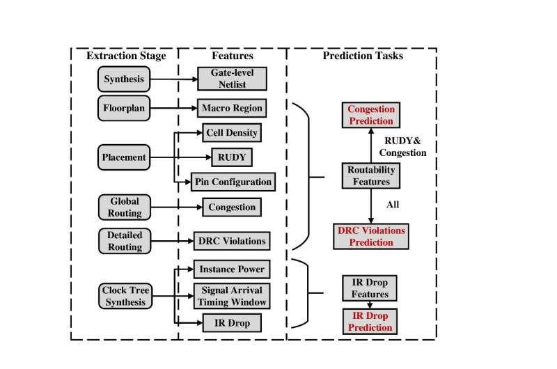
Overall flow for data collection and feature extraction. Credit: Science China Press
To address this issue, the research group from Peking University has released the first open-source dataset, called CircuitNet, which is dedicated to AI for IC applications in VLSI CAD. The dataset consists of over 10K samples and 54 synthesized circuit netlists from six open-source RISC-V designs, provides holistic support for cross-stage prediction tasks, and supports tasks including routing congestion prediction, design rule check (DRC) violation prediction and IR drop prediction. The main characteristics of CircuitNet can be summarized as follows:
- Large scale: The dataset consists of more than 10K samples extracted from versatile runs of commercial EDA tools with commercial PDKs (currently in 28nm technology node, and will support 14nm technology soon).
- Diversity: Different settings in logic synthesis and physical design are introduced to reflect diverse situations in the design flow.
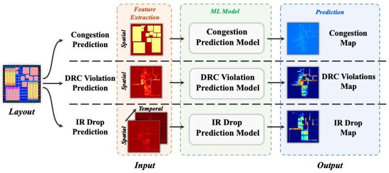
- Multiple tasks: The dataset supports three prediction tasks, i.e., congestion prediction, DRC violation prediction, and IR drop prediction. The dataset includes features widely adopted in the state-of-the-art methods and is validated through experiments.
- Easy-to-use formats: Features are preprocessed and transformed into Numpy arrays with restricted information removed. Users can load the data easily through Python scripts.
Three cross-stage prediction tasks: congestion, DRC violations, and IR drop. Credit: Science China Press
To evaluate the effectiveness of CircuitNet, the authors validate the dataset by experiments on three prediction tasks: congestion, DRC violations, and IR drop. Each experiment takes a method from recent studies and evaluates its result on CircuitNet with the same evaluation metrics as the original studies. Overall, the results are consistent with the original publications, which demonstrates the effectiveness of CircuitNet. A detailed tutorial about the experimental setup is available on GitHub. In the future, the authors plan to incorporate more data samples with large-scale designs in advanced technology nodes to improve the scale and diversity of the dataset.


