Chinese semiconductor industry

Status
Not open for further replies.

supersnoop

Major
Registered Member
It takes time for a process to mature and for production to be the raised. In the GT article, that expert said

He sounded pretty confident about it there about 7 nm and also 5 nm. And he is saying basically they have already finished all the work they needed for 14 nm and that they have moved onto 7 nm. His comment sounds like their yield on 7 nm is now acceptable. So, you have to ask yourself if 7 nm here is referring to N+1 process or the N+2 process (which is close to the earliest Samsung 5nm but SMIC calls 7 nm).


It shouldn't be that hard to procure equipment for 14 nm process, right? I'm interpreting this as not getting the equipment for ramping up more advanced nodes. I hope the purchase of all these NXT 2050i means they are confident that they have all that they need to ramp up production. It would be silly to have a bunch of DUVs ready for N+1/N+2. They must have paid some good money for ASML to develop more powerful NXT 2050i and 2100i just for them. I mean after all, the report explicitly said "for the most critical layers". So, that means these will be used like EUVs in SMIC's process.


I don't know. I just know they are really ramping up their production in those large 12 inch megafabs. SMIC/YMTC/CXMT/HuaHong/CanSemi/Silan all have plenty of large expansion projects. How much domestic market share they can occupy really depends on the economy and China's continued industrialization.

I think it's pretty important to get to more advanced nodes. For example, they've been building super computers using Phytium's S2500 server chips and need like 750k of them per super computer. If they can move Phytium server chips to N+1 or N+2 process, that will increase the power of their super computers. Similarly, they need N+1 chips to have more powerful fully domestic desktops that can replace foreign computers in organizations with sensitive info.

I did a calculation yesterday. For every 10k wpm of N+2 improved production, they can produce about 80 million smartphone CPUs a year. To put things into perspective, Xiaomi sold 190 million phones last year. So if they want to support Huawei, they'd need to dedicate probably 30k wpm of N+2 production just to provide enough Kirin chips to support Huawei returning to its former sales numbers. In reality, the demand from Chinese smartphone makers is probably closer to 600 million a year right now and growing. That would be 80k wpm of their most advanced process. Which is more than the planned capacity of SN1/SN2 combined.

So, SMIC need more advanced node fab.

Even N+1 will make a huge difference in smartphone volume. Only the high end phones (Apple, Mi Pro, Samsung Galaxy S) are using 5nm chips. Many mid range are still on 7nm and that is a big chunk of the market, especially non western ones. The lowest end phones using UNISOC are even 14nm.
 

tokenanalyst

Brigadier
Registered Member

Xu Min's research group from the School of Microelectronics proposed a gate-last single-diffusion process integration solution for advanced process nodes of 3nm and below to meet the N/P current matching challenge in gate-all-around transistors​


Compared with fin transistors (FinFETs), the vertically stacked gate-all-around nanosheet transistor (GAA NS-FET) architecture has superior channel control capability, larger drive current per unit area, and tunable nanosheet widths. It is another important process technology change after FinFET; Samsung, TSMC, and Intel have launched fierce competition in GAA process technology. For GAA NS-FET, the channel direction remains the same as <110>, while the main transport surface direction changes from (110) to (100), which brings a great challenge to GAA technology: unlike FinFET’s (110) ) conducting plane, the (100) plane has higher electron mobility but lower hole mobility, which makes the N/P current matching characteristic in FinFET very difficult to achieve in GAA. In addition, due to the discontinuity of the source-drain epitaxial surface in the GAA, it is difficult for the epitaxial SiGe source-drain in the p-FET to effectively stress the p-type channel. Therefore, how to enhance the stress of the p-type channel has become the most critical technology to achieve N/P current matching in GAA.

In response to the above problems, Zhang Wei/Xu Min's research group from the School of Microelectronics of Fudan University innovatively proposed a gate-back-single-diffusion (PG-SDB) process integration scheme based on the self-built DTCO simulation platform. Single-diffusion (SDB) and self-aligned single-diffusion (SA-SDB), PG-SDB can significantly increase channel stress for N/P current matching. The related work was published in IEEE Transactions on Electron Devices under the title of "Novel Post-Gate Single Diffusion Break Integration in Gate-All-Around Nanosheet Transistors to Achieve Remarkable Channel Stress for N/P Current Matching" . Liu Tao, a postdoctoral fellow in the School of Microelectronics, is the first author, and Professor Zhang Wei, researcher Xu Min, and young researcher Wu Chunlei are the co-corresponding authors.

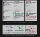
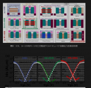
Compared with the traditional SDB and SA-SDB process integration solutions, the PG-SDB process integration solution proposed in this paper realizes the SDB process module after replacing the metal gate (RMG) process (Fig. 1), which can effectively eliminate the stress relaxation on the free surface. (figure 2). Further analysis shows that the proposed PG-SDB process integration scheme not only avoids the stress relaxation of the free surface, but also obtains additional stress enhancement from the dummy gate region (Fig. 3), significantly boosting the channel stress to +3.5 GPa (n-type channel)/-4.7 GPa (p-type channel). Further electrical simulation results show that better drive capability and N/P current matching are achieved in the GAA NS-FET device integrated with the PG-SDB process scheme (Figure 4). Therefore, the proposed PG-SDB process integration scheme has great application potential in 3nm GAA CMOS technology and beyond.

1663436336911.png1663436365805.png

Please, Log in or Register to view URLs content!
 

4Runner

Junior Member
Registered Member
If they can achieve commercially viable yields on this 7nm GPU design in the next 18-24 months, no matter how good/bad the design actually is, it will turn out to be yet another watershed event. Generally speaking, if they can make a decent GPU, even in the low/medium range of Nvidia/AMD mainstream lines, they definitely can build a GPGPU off that GPU design. Forget about the graphics card market. GPGPU for supercomputing and AI applications is the real deal. A made-in-China GPGPU at 7nm, even around 2024/2025 with commercially viable yields, would essentially break up all bleeding edge sanctions. From that point on, it would be US in general and Nvidia/AMD in particular really worry about their future in high-performance computing.
 

tphuang

Lieutenant General
Staff member
Super Moderator
VIP Professional
Registered Member
Please, Log in or Register to view URLs content!

Looks like Sberbank has awarded an $128 million contract to a Chinese server provider (Lenovo, Inspur or Huawei). It's unclear to me what chip they will be using here. I don't think Huawei can use Kunpeng chips unless they developed a process with SMIC recently. It's doubtful that either Lenovo or Inspur would be using American server chips. So they most obvious answer is for them to offer Phytium's S2500 server.

If this is true, it certainly makes sense for Russian companies to turn to Chinese tech companies for their ICT solutions. Now, let's see if China can start exporting Chinese chips to other SCO countries and ASEAN countries.

If they can achieve commercially viable yields on this 7nm GPU design in the next 18-24 months, no matter how good/bad the design actually is, it will turn out to be yet another watershed event. Generally speaking, if they can make a decent GPU, even in the low/medium range of Nvidia/AMD mainstream lines, they definitely can build a GPGPU off that GPU design. Forget about the graphics card market. GPGPU for supercomputing and AI applications is the real deal. A made-in-China GPGPU at 7nm, even around 2024/2025 with commercially viable yields, would essentially break up all bleeding edge sanctions. From that point on, it would be US in general and Nvidia/AMD in particular really worry about their future in high-performance computing.
hmm, China already has Kunlun, BR100/104, Hanbo Semiconductor chips, Cambrian, Tianshu Zhixin and many others. This is really not a big deal anymore.

I'd be more concerned about how quickly Kunlun and Biren technology can get a chip designed with SMIC's N+2 process. Since SMIC's roadmap calls N+2 their 7 nm chip (even though it's performance is close to the earliest Samsung 5 nm chip), I think we should we will see the Chinese chip designers using SMIC process very soon. This just indicates that SMIC is already working with domestic AI/Server GPU/CPU players to design their chips. That's very important.

I was wondering why I have not heard of Wuxi before. It turns out that they didn't get started until Sep 2020. That's probably why it's taking so long to be ready.
 

hhuang41

New Member
Registered Member
Story and data is weird and contradictory to all other news regarding domestic substitution, but it is an important topic so deciding to share.
Please, Log in or Register to view URLs content!
"China’s monthly
Please, Log in or Register to view URLs content!
output recorded its biggest ever decline in August, as the government’s
Please, Log in or Register to view URLs content!
and a
Please, Log in or Register to view URLs content!
continued to
Please, Log in or Register to view URLs content!
.
Production of integrated circuits (ICs) last month slumped 24.7 per cent year on year to 24.7 billion units, marking the largest single-month decrease since records began in 1997, according to data released by the National Bureau of Statistics (NBS) on Friday. The IC volume was the lowest on record since October 2020.
That also marked the second consecutive month of contraction for the domestic semiconductor industry, which saw its output
Please, Log in or Register to view URLs content!
."
 
Status
Not open for further replies.
Top