Tunability is a nice idea in theory but in practice your projection optics are paired to very specific wavelengths, especially at shorter wavelengths where the spectral range for good optics pairings become very narrow. This means you will need dedicated projection system for each wavelength you intend to use, and it may not be the case that you will have materials that can do projection of your light output for all the wavelengths you’d be interest in without a level of photon loss that might make those wavelengths impractical, or at least subject to higher light output requirements.Very interesting!
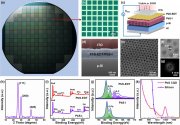
- In this work, a 2.5 × 2.5 mm2 large-area 4H-SiC Schottky barrier photodiode with a grid-shaped semitransparent metal electrode is designed and fabricated for extreme ultraviolet (EUV) detection
- Based on a synchrotron radiation source, the photo-response characteristics of the photodiode is measured between 5nm and 140nm
- EUV detectors are the key component used for monitoring and calibrating photon beam intensity
So, this was obviously used for testing EUV light, sourced from either the SSMB or SSRF, or both. Even more interesting that 5nm-140nm wavelengths were tested. Unlike LPP generated EUV, synchrotrons can easily tune the wavelength and in a very real sense make up for photoresist sensitivity that might be most optimal for wavelengths other than 13.5nm. Imagine using 11.2nm instead of 13.5nm and realizing <7nm features using the same 7nm process. Conversion efficiency isn't as big an issue so tuning the wavelength would achieve what would otherwise need lithium powered LPP EUV.
On a related note, does anybody know how photoresists would react with uber powered synchrotron generated EUV source power in the multi-kilowatt range? I imagine a synchrotron driven EUV litho machine would simply run faster. With that much power, photoresist parameters could be looser such that photoresists would be an easier bottleneck to crack vs photoresist designed for much lower powered EUV light sources. Photoresist over-exposure might also become an issue on the flip side so comments to this are appreciated.
You are using an out of date browser. It may not display this or other websites correctly.
You should upgrade or use an alternative browser.
You should upgrade or use an alternative browser.
Chinese semiconductor industry
- Thread starter Hendrik_2000
- Start date
- Status
- Not open for further replies.
According to various reports, China bought 81 Arfi lithography machines last year. If we add another 40 in first half of this year, that's 120 in the past 18 months. Which would support 12 * 50k = 600k wafers of 28 nm per month or 300k wafers of 7 nm per month. That seems to be way beyond what China is adding this year, which makes me think they might be stocking up before a ban comes through.
Keep in mind that one way around the slower production rate that multi patterning imposes is to get more scanners into your production line. I think this is more a signal that they’re expecting to expand production that uses multipatterning than a linear signal of how much wafer capacity they intend to bring aboard.
That's why Molybdenum-Silicon dialectric mirrors are used for optimal reflectivity at 13.5nm. At 11.2nm, Molybdenum-Beryllium is used for that wavelength for the same reason. Going below 11.2nm is not feasible unless we do away with mirrors to use some sort of direct exposure system. I've always wondered how this could be done with X-Ray lithography. Russia recently announced they were working on synchrotron X-Ray based lithography without the need for mirrors or photomasks. I haven't investigated it but it sounds sort of like electron beam lithography. Their aim is to use this for directly fabbing circuits vs making photomasks for traditional photolithography like EBL.Tunability is a nice idea in theory but in practice your projection optics are paired to very specific wavelengths, especially at shorter wavelengths where the spectral range for good optics pairings become very narrow. This means you will need dedicated projection system for each wavelength you intend to use, and it may not be the case that you will have materials that can do projection of your light output for all the wavelengths you’d be interest in without a level of photon loss that might make those wavelengths impractical, or at least subject to higher light output requirements.
Yes, but nonetheless we’re talking about an additional projection system for each target wavelength. I think if SSMB is treated as infrastructure vs equipment your optics systems can be modularized, but it’s still an extra condition that will constrain (significantly I think) just how much tunable range you can use.That's why Molybdenum-Silicon dialectric mirrors are used for optimal reflectivity at 13.5nm. At 11.2nm, Molybdenum-Beryllium is used for that wavelength for the same reason. Going below 11.2nm is not feasible unless we do away with mirrors to use some sort of direct exposure system. I've always wondered how this could be done with X-Ray lithography. Russia recently announced they were working on synchrotron X-Ray based lithography without the need for mirrors or photomasks. I haven't investigated it but it sounds sort of like electron beam lithography. Their aim is to use this for directly fabbing circuits vs making photomasks for traditional photolithography like EBL.
Have to distinguish hard vs soft X-rays. Hard X-rays (10s to 100s keV) use grazing incidence and diffraction based optics or specialized absorber materials due to the very close to 1 coefficient of refraction in most materials and relatively low absorbance. Their photon energy is in a region with energy too low for nuclear scattering and too high for core electron photoionization, so their absorption cross section is relatively low.That's why Molybdenum-Silicon dialectric mirrors are used for optimal reflectivity at 13.5nm. At 11.2nm, Molybdenum-Beryllium is used for that wavelength for the same reason. Going below 11.2nm is not feasible unless we do away with mirrors to use some sort of direct exposure system. I've always wondered how this could be done with X-Ray lithography. Russia recently announced they were working on synchrotron X-Ray based lithography without the need for mirrors or photomasks. I haven't investigated it but it sounds sort of like electron beam lithography. Their aim is to use this for directly fabbing circuits vs making photomasks for traditional photolithography like EBL.
Soft X-rays (1-10 keV) are more like EUV, because they're highly absorbed by deep core electrons in core photoionization (just like EUV is highly absorbed by outer core electrons and VUV is highly absorbed by valence electrons due to energy level matching the photoionization energy of those orbitals).
Grazing incidence optics severely limits possible optical configurations and focusing, which is why X-ray lithography is so hard, and soft X-rays lithography doesn't have significant advantage over EUV because it has similar problems but is harder to make a resist for.
Diffraction optics is also terrible for photon count. With illumination lithography your key metric is the photon dose, because photon dose drives scanning speed. If you can’t get scanning speed up you’re not commercially viable.Have to distinguish hard vs soft X-rays. Hard X-rays (10s to 100s keV) use grazing incidence and diffraction based optics or specialized absorber materials due to the very close to 1 coefficient of refraction in most materials and relatively low absorbance. Their photon energy is in a region with energy too low for nuclear scattering and too high for core electron photoionization, so their absorption cross section is relatively low.
Soft X-rays (1-10 keV) are more like EUV, because they're highly absorbed by deep core electrons in core photoionization (just like EUV is highly absorbed by outer core electrons and VUV is highly absorbed by valence electrons due to energy level matching the photoionization energy of those orbitals).
Grazing incidence optics severely limits possible optical configurations and focusing, which is why X-ray lithography is so hard, and soft X-rays lithography doesn't have significant advantage over EUV because it has similar problems but is harder to make a resist for.
My understanding is that the optics system would remain the same. Synchrotron wavelength could be tuned by adjusting the electron energy. This is done anyways with SSMB, so using 13.5nm or 11.2nm or other wavelengths would need the same setup. The main difference would be the Bragg mirrors which would be more difficult to manufacture Molybdenum-Beryllium for 11.2nm Such mirrors need more layers than Mo:Si and a challenge considering how toxic it is.Yes, but nonetheless we’re talking about an additional projection system for each target wavelength. I think if SSMB is treated as infrastructure vs equipment your optics systems can be modularized, but it’s still an extra condition that will constrain (significantly I think) just how much tunable range you can use.
Do Mo-Be mirrors cover both 11.2 and 13.5 wavelength ranges? What are their transmission efficiencies for each? Will light from the two wavelengths exhibit the same scattering behaviors using the same mirrors and optical configurations? You have to factor all that in. Optical systems are very precise instruments, and nanoscale lithography requires extremely unforgiving tolerances.My understanding is that the optics system would remain the same. Synchrotron wavelength could be tuned by adjusting the electron energy. This is done anyways with SSMB, so using 13.5nm or 11.2nm or other wavelengths would need the same setup. The main difference would be the Bragg mirrors which would be more difficult to manufacture Molybdenum-Beryllium for 11.2nm Such mirrors need more layers than Mo:Si and a challenge considering how toxic it is.
Last edited:
Mo:Be is optimal for 11-12.4nm with similar scattering to Mo:Si. Mo:Si is optimal for 12.4-14nm. I believe 13.5nm was chosen for the reasons you insinuate here. Primarily because Mo:Be reflectivity is significantly lower than Mo:Si at the target wavelengths of 11.2nm and 13.5nm respectively. Also, the conversion efficiency using Tin is nearly double that of what they were experimenting with 10+ years ago with Xenon, Lithium or various doped combinations to get to 11.2nm. What changes this calculation is that synchrotrons can produce so much power that it overwhelms what were considered roadblocks in the past. That doesn't mean the SSMB will absolutely settle on 11.2nm vs 13.5nm but the reasons to do so are compelling. My hope is that SSMB EUV lithography will eventually see the light of day because if it does, I believe it will be the end of what I consider 1 of the 3 remaining pillars of American allied power.Do Mo-Be mirrors cover both 11.2 and 13.5 wavelength ranges? What are their transmission efficiencies for each? Will light from the two wavelengths exhibit the same scattering behaviors using the same mirrors and optical configurations? You have to factor all that in. Optical systems are very precise instruments, and nanoscale lithography requires extremely unforgiving tolerances.
- Status
- Not open for further replies.


