Chinese semiconductor industry

Status
Not open for further replies.

tokenanalyst

Brigadier
Registered Member

Xinrui Micro received tens of millions of yuan in A+ round of financing to develop EDA physics simulation software tools around the Chiplet industry​


Recently, Xinrui Micro completed tens of millions of RMB A+ round of financing, invested by Zhongke Chuangxing, and Fengliu Capital served as the exclusive financial advisor. This round of financing will be mainly used for R&D team expansion, as well as industrial integration and company mergers and acquisitions.

1096155748867.022265482085284.64157.png


Founded at the end of 2019, Xinrui Micro has a team size of nearly 60 people, with R&D personnel accounting for 80%. The core teams are from world-renowned EDA and industrial software companies. The core members have an average of nearly 30 years of R&D experience in the simulation field. The company focuses on the field of EDA physical simulation, and develops a multi-physics system simulation platform that integrates multiple functional modules such as electromagnetic, electrothermal, DC, magnetic loss, stress, fluid, etc., to further fill the gap in the domestic system simulation field. At the same time, the company can also provide customers with one-stop solutions such as wafer-level packaging design and foundry services, IC beta design services, advanced packaging design services, and board-level hardware design services.

As Moore's Law is gradually approaching the physical limit, it is difficult for the industry to achieve a jump in chip performance by doubling the number of transistors. Therefore, many players have begun to try to find new paths from the perspective of packaging, board level, and system level to achieve Moore's Law. Continuation . Under this trend, Chiplet technology, which has the advantages of high performance, low power consumption, high area utilization and low cost, has been paid more and more attention.

Not only that, the shortage of advanced chip production capacity and the tense global environment have accelerated the rapid outbreak of the chiplet field. According to Omdia data, the global chiplet market is expected to reach $5.8 billion by 2024, and this figure will grow to $57 billion by 2035.

The rapid development of chiplet technology has brought new opportunities to the EDA field. In the field of Chiplet design, multi-physics simulation tools that can perform multi-physics simulation analysis for heterogeneous integration and 3D stacking systems, and can provide guidance for design and material selection have become a necessity and the main development of a new generation of EDA. direction.

But challenges are also evident. Guo Ru, founder and CEO of Xinrui Micro, said that in industrial software and EDA tools, simulation tools can be called tools within tools, which need to simulate accurate reality without knowing the real data. In this simulation process, it puts forward higher requirements on the algorithm, architecture, and overall simulation accuracy and performance. "The difficulty of a simulation tool is that it must not only simulate accurately, but also guide the design. It is the most difficult link in the entire industrial software and EDA chain. We hope to continue on this difficult and correct path." She Say.

Since its establishment at the end of 2019, Xinrui Microelectronics has successfully developed four products, including electromagnetic simulation, electrothermal simulation, DC analysis, and thermal circuit extraction, which have been commercialized. Among them, the company's electromagnetic simulation products have laid a solid foundation for other customers to do product migration through in-depth research and development cooperation with leading domestic customers.

For example, in high-density, high-integration electronic equipment, signal integrity and power integrity problems are prominent, and temperature and heat dissipation have become the core problems of the industry. In order to achieve higher performance requirements, the interconnection method must be optimized with the help of electromagnetic, electrothermal and other physical field simulation tools, and the verification and assistance of the optimized design can guide the design and ensure system performance. Based on this, the company's electromagnetic, electrothermal and multiphysics simulation software can provide customers with high-quality, high-reliability design simulation services.

At the same time, in June this year, Xinrui Micro completed the wholly-owned acquisition of Shenzhen Zhongke System Integration Technology Co., Ltd. (referred to as "Shenzhen Zhongke"). Shenzhen Zhongke is a one-stop comprehensive service provider for advanced system-in-package design. Shenzhen Zhongke was established in 2011 and will transplant its industrial accumulation to the Chiplet field in 2021.

Through this acquisition, on the one hand, Xinrui Microelectronics has become an overall solution provider that integrates Chiplet one-stop service with domestic system simulation EDA tools and simulation processes as the core; on the other hand, the company has also completed the complementation of customer types, realizing The number of customers has increased exponentially, further improving the company's sales layout and providing customers with overall solutions.

Guo Ru said that the entire EDA chain can be roughly divided into two parts: chip design EDA and system design EDA. Among them, many domestic players are currently in the field of chip design EDA, such as front-end design, back-end layout and wiring, logic simulation, etc. "Every sector is very difficult, especially in the field of simulation." She explained that Xinrui's simulation software is not only limited to the chip, but more on the packaging and system side, without relying on the maturity of Foundry's advanced process, And it has become an essential EDA tool for design in the chiplet field.

This means that before the domestic advanced process is put into mass production, the company can use simulation methods to help domestic industries use mature 28nm chips and 3D stacking methods to produce equipment and products with more advanced performance. "That is to say, within 5-10 years, we can provide the opportunity to overtake on the curve and break Moore's Law. This is the fundamental reason why we can quickly achieve commercialization, and it is also our differentiated competitive advantage." Guo Ru said.

Therefore, Xinrui will be based on the coupling of single-point tools such as electromagnetic and electrothermal and multi-physics in product planning. Based on this layout, the company's products will first be suitable for commercial customers in terms of landing, and then cooperate with professional vertical customers to accelerate the landing process.

Please, Log in or Register to view URLs content!
 

ansy1968

Brigadier
Registered Member
From SCMP, I never heard of this company, one of the 10,000 tech SME?

Tencent-backed start-up Jaguar Microsystems bets on chip innovation to help propel growth of China’s cloud computing market​

  • JaguarMicro develops advanced data processing units, a new class of programmable chips, for servers used in data centres
  • The Shenzhen-based tech unicorn expects to record annual revenue of more than US$1 billion in three years

Please, Log in or Register to view URLs content!


Please, Log in or Register to view URLs content!

+ FOLLOW
Published: 10:00pm, 12 Sep, 2022


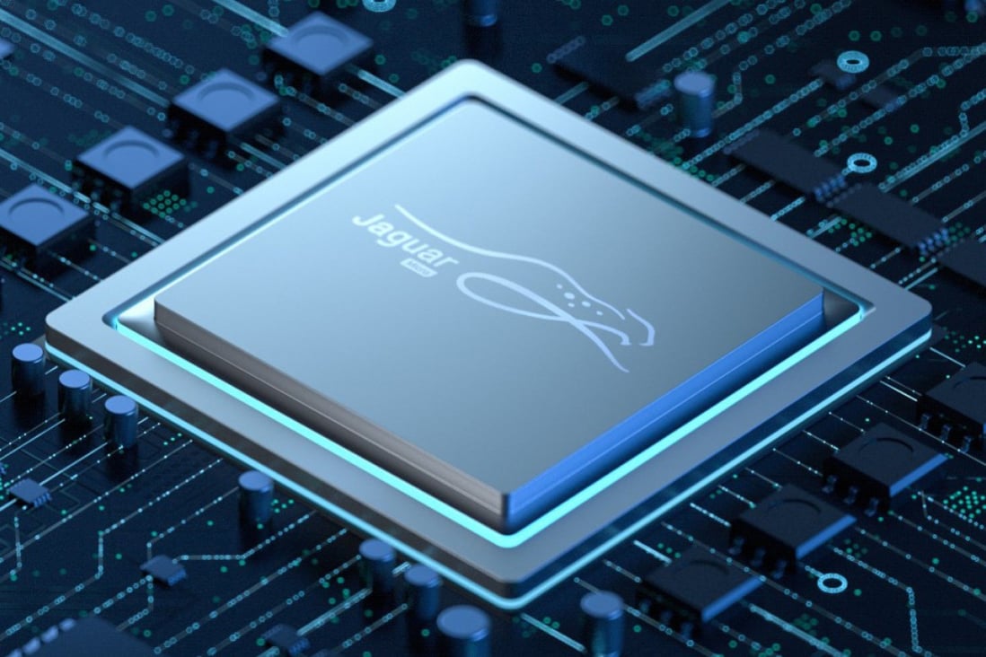
Tech unicorn Jaguar Microsystems is focused on developing the most advanced data processing units for servers used in data centres. Photo: Handout

Tech unicorn Jaguar Microsystems is focused on developing the most advanced data processing units for servers used in data centres. Photo: Handout
Please, Log in or Register to view URLs content!
-backed
Please, Log in or Register to view URLs content!
Jaguar Microsystems (JaguarMicro) is seeking to become a major technology supplier to China’s fast-growing
Please, Log in or Register to view URLs content!
services market with its innovative new chips, providing a beacon of light to the country’s
Please, Log in or Register to view URLs content!
industry amid growing tensions between Beijing and Washington.
Please, Log in or Register to view URLs content!
-based JaguarMicro is focused on developing data processing units (DPUs), a new class of programmable systems-on-a-chip, for servers used in
Please, Log in or Register to view URLs content!
, Hong Kong-born Sunny Siu, the company’s founder, chairman and chief executive, said in a recent interview.
“Like electricity, cloud computing will become a new utility,” Siu told the South China Morning Post. “And our goal is to help the utility providers cut their costs, while increasing their output.”
Cloud computing services enable companies to buy, sell, lease or distribute a range of software and other digital resources as an on-demand service over the internet, just like electricity from a power grid.
Sunny Siu, the founder, chairman and chief executive of Shenzhen-based Jaguar Microsystems. Photo: Handout

Sunny Siu, the founder, chairman and chief executive of Shenzhen-based Jaguar Microsystems. Photo: Handout
Those resources are managed inside data centres, which are secure, temperature-controlled facilities built to house large-capacity servers and data storage systems linked to multiple power sources and high-bandwidth internet connections.

“China’s cloud computing market is booming,” Siu said. That is why he expects JaguarMicro to record annual revenue of more than US$1 billion in three years.

China’s industrial and manufacturing sectors will be able to
Please, Log in or Register to view URLs content!
in the country’s cloud computing market, according to a recent report by global management consulting firm McKinsey & Co. It forecast China’s public cloud services market, which is already the world’s second-largest behind the
Please, Log in or Register to view URLs content!
, to reach US$90 billion in revenue by 2025, up from US$32 billion in 2021.

DPUs are expected to join traditional central processing units (CPUs) and graphics processing units (GPUs) to become the three pillars of computing, according to
Please, Log in or Register to view URLs content!
, the co-founder, president and chief executive of Nvidia Corp.

Please, Log in or Register to view URLs content!

Unlike CPUs and GPUs in which
Please, Log in or Register to view URLs content!
and Nvidia have already built up clear advantages in the global semiconductor industry, the DPU market is still in its infancy and has many new businesses jostling to set industry standards and benchmarks.
Demand for JaguarMicro’s DPUs is expected to be driven by its innovation for processing networking, storage, virtualisation and security applications. That frees up a server’s CPU to handle other workloads and help cloud platform operators become more efficient and cut costs, Siu said.


Founded in 2020, JaguarMicro has become one of the hottest companies for investors in the DPU market and raised more than US$200 million from a financing round early in 2021, making it a tech unicorn with a valuation of more than US$1 billion. Tencent has a 24 per cent stake in JaguarMicro, which also has the likes of Sequoia Capital China,
Please, Log in or Register to view URLs content!
, the
Please, Log in or Register to view URLs content!
and various other venture capital firms as investors.

Siu and his core team at JaguarMicro each have more than 20 years of experience in the semiconductor industry. Its world-class silicon and software team includes personnel who previously worked at companies that include
Please, Log in or Register to view URLs content!
, Intel,
Please, Log in or Register to view URLs content!
,
Please, Log in or Register to view URLs content!
and
Please, Log in or Register to view URLs content!
, the chip design unit of
Please, Log in or Register to view URLs content!
. Alibaba owns the Post.
Aerial view of the Hong Kong Science Park in Pak Shek Kok, an area located at Tai Po district in the New Territories. Photo: Roy Issa

Aerial view of the Hong Kong Science Park in Pak Shek Kok, an area located at Tai Po district in the New Territories. Photo: Roy Issa
Siu, who holds a doctoral degree from Stanford University, served as president of ProphetStor Data Services, a cloud solutions provider he co-founded in California, before taking the helm at JaguarMicro. Siu had also worked for three years as Greater China managing director for Broadcom’s processor unit from 2012 to 2015 after the US firm acquired NetLogic Microsystems, where he previously served as president and Asia-Pacific general manager.
 

ansy1968

Brigadier
Registered Member
continue....

JaguarMicro’s recent expansion, which includes setting up its international operations at the
Please, Log in or Register to view URLs content!
, offers a glimmer of hope for China’s semiconductor industry amid the sense of urgency brought by recent actions of the US government.
Earlier this month, Washington
Please, Log in or Register to view URLs content!
used for
Please, Log in or Register to view URLs content!
and high-performance computing work to China.
In August,
Please, Log in or Register to view URLs content!
on technologies for the production of advanced chips were imposed by the US government.

Still, those developments have not deterred JaguarMicro’s business development programme. The firm, which currently has more than 400 employees, opened a new research and development centre last month at the Hong Kong Science Park.​

Siu said the biggest roadblock for future growth is a talent crunch, which is the reason JaguarMicro expanded to Hong Kong. “There is a lot of world-class talent in Hong Kong, but they need more cultivation,” he said, adding that the company hopes to contribute to transforming the city into an international innovation hub.
 

european_guy

Junior Member
Registered Member
Bro Epic really epic especially 3 and 4, what about Europe the answer, none of the above, they become irrelevant...lol

Bro, Europe is completely out of these games.

The main actors in European semiconductor world (ST, Infineon, NXP, AMS) are mainly focused on automotive / industrial applications, so in MCU and power devices. Although their portfolio is quite wide, this is their core business.

IMO they already know they will loose the Chinese market, but due to decades old strong partnership with Eurpean automotive and industrial companies, they still think to have a comfortable future as long as they are cautious with investments and keep financial books in order...and European automotive industry does not collapse.

Europe does not have hegemonic mentality, nor its people, nor its companies. We just aim at a comfortable and healthy life :) we try to keep ourselves away from troubles....
 

tokenanalyst

Brigadier
Registered Member

Anhui Dahua Semiconductor Technology Co., Ltd.: providing intelligent packaging systems for the semiconductor integrated circuit industry​


Founded in June 2014, the company is a high-tech enterprise that provides intelligent packaging systems, precision molds and other products for the semiconductor integrated circuit packaging and packaging and testing industries . It is located in the Technology Industrial Park of Hefei High-tech Zone. With a modern production plant of nearly 10,000 square meters, it has introduced advanced equipment at home and abroad such as surface grinders, high-speed milling machines, EDM machines, fast and slow wire cutting, gantry surface grinders, CNC washers, measuring microscopes, and three-coordinate measuring machines. . An advanced mold production and testing center and two integrated circuit automatic flexible assembly production lines have been built.

The company has established a complete system and has passed IS9001, ISO14001 and intellectual property system certification. The company has successively been identified as: national high-tech enterprises, "specialized, refined and new" small and medium-sized enterprises in Anhui Province, "specialized, refined and new" small and medium-sized enterprises in Hefei, Hefei intellectual property demonstration enterprises, high-tech zone science and technology giant enterprises, high-growth enterprises - Gazelle Cultivation Enterprise, the second prize of the 2020 "Maker China" SME Innovation and Entrepreneurship Competition Finals, and the winner of the "Excellence Award" in the Hefei Division of the 9th China Innovation and Entrepreneurship Competition. The self-developed "120T integrated circuit automatic packaging system equipment, 180T chip-level automatic plastic packaging system vehicle T0252 vacuum packaging and molding system" are respectively known as the first (set) major equipment in Anhui Province in 2017, 2018 and 2019.

Currently successfully developed and sold products include: integrated circuit automatic packaging system, integrated circuit rib cutting and bending automation system, servo hydraulic press, various auxiliary equipment for semiconductor post-process and various precision molds, such as mold boxes, rib cutting stamping dies , MGP mold, etc.

Dahua Technology adheres to the business philosophy of " product innovation, efficient service, and bilateral win-win ". In-depth exploration of customer needs, continuous introduction of innovative products that fit the market, and gradual expansion of market visibility and market share are the company's driving forces; serving customers, solving practical problems encountered in design and production for customers, so that customers can be more convenient and more assured Using the company's products is the goal of the company's constant focus; dare to be the first, make the best products in China, and create the greatest value for users! Inject core power into Chinese enterprises!

Please, Log in or Register to view URLs content!

Jiu Zong intelligent semiconductor testing equipment production project was successfully signed in Anhui​

Recently, the Jiuzong intelligent semiconductor testing equipment production project with a total investment of about 100 million yuan was officially signed in Xiuning County, Anhui Province.

It is understood that the project is invested and constructed by Ningbo Jiuzong Intelligent Technology Co., Ltd., which is a high-tech company founded by experts in the national optical field. It mainly develops and produces 3D measurement, AOI appearance inspection, and inspection AI automation in the 3C and semiconductor fields and other equipment. The project is located in Xinping New Material Industrial Park, Xiuning Economic Development Zone. It is constructed in three phases. After the project is fully completed, the annual output value will reach 180 million yuan, and the annual tax will be about 5 million yuan.
 

tphuang

Lieutenant General
Staff member
Super Moderator
VIP Professional
Registered Member
Not sure how he determines it is much lower performance than SS/TSMC without actually having tested the chip himself. The SMIC N+1 has 89 PPA vs around 60 PPA for TSMC/Samsung 10 nm. It's pretty close to the first gen Samsung 7nm chip.

Based on
Please, Log in or Register to view URLs content!
, it seems like N+1 process have technology from 10 nm and 7 nm and probably works well enough for domestic desktop/server CPU producers that is looking for something that's better than 14 nm right now.

As for capacity, this came out last year
Please, Log in or Register to view URLs content!
SMIC revealed in May last year that the total investment planned for the Shanghai wafer plant was $9.06 billion.
As of May last year, SMSC was capable of making 6,000 14-nm wafers per month, but it wants to reach a manufacturing capacity of 35,000 units per month for 14-nm and below wafers, according to a filing by the Hong Kong-listed company.

“SCMC’s planned capacity of 35,000 per month is about 10% of the world’s 14nm manufacturing capacity,” Geng Chen, an analyst from Hua Chuang Securities, said. Besides 14nm, SMIC’s more advanced nodes, 12nm and N+1, have also started mass production, as revealed by co-chief executive Liang Mong-Song in December. Liang said the company had finished developing the 7nm process and planned for trial mass-production in April 2021, plus development of 5nm and 3nm production in the future.
Please, Log in or Register to view URLs content!
Semiconductor Manufacturing International Corporation's (SMIC) FinFET process is in production and has a capacity of 15,000 wafers per month
Please, Log in or Register to view URLs content!
Looking at page 163 of their annual report for 2021. Looks like SMSC generated $691 million in revenue in 2021 compared to $139 million in 2022. Which means they probably were generating $20 million a month at start of the year and $100 million per month by the end. They reached 15k wpm by August of last year and probably significantly more than that by end of the year with all the ASML DUVs they've been taking in.

Now, if we compare that to SMNC, which generated $1.5 billion in 2021 vs under $1 billion in 2020. Assuming that SMNC fully reached 100k wpm in 2021, then they probably generated $120 to 140 million a month for SMNC fab. It seems to me that 35k wpm in advanced nodes should generate more revenue per month than 100k wpm of 28 to 65 nm nodes, because they invested $9 billion to build this fab vs $7.5 to $8.5 billion they invested in 100k wpm fabs. As such, there is likely more room for revenue generation at SMSC fab from both more advanced nodes and higher capacity.

It would make sense that SMIC started trial mass production of N+1 node in Q2 of 2021 since this much discussed mining ASIC chip was form last year. Maybe, they were test trialing it with some less important products first. It's like that that 2022 is the first full year they have started producing large amount of N+1 chips. 2023 is likely the first year they do mass production of N+2.

Quoting @tinrobert's article
Please, Log in or Register to view URLs content!

about twice as many DUVs and masks are needed to produce 7 nm vs 28 nm (maybe a little more than twice). If SMIC's N+2 and N+2 improved nodes are close to 5 nm (and even Samsung 4 nm), then maybe they will need 3 times as many DUVs and masks to produce. As such, I would guess the 35 wpm is measured based on how many of N+2 nodes that fab could theoretically produce down the road. And if they can produce 35 wpm of N+1/N+2 chips at this 1 plant, it would be a pretty big deal.
 

european_guy

Junior Member
Registered Member

Official ASML financial report for first half of 2022​


Please, Log in or Register to view URLs content!

Some highlights:

1) "With regards to new lithography systems, we recognized revenue for 127 DUV and 15 EUV systems in the first half of 2022, compared to 126 DUV and 16 EUV systems in the first half of 2021"

2) "DUV – Continuing innovation in our latest-generation immersion system NXT:2050i and introduction of the dry system
XT:860N. Continued developments for the next generation of scanners, NXT:2100i for the most critical DUV layers, and
NXT:870 for break-through productivity in the KrF dry market. We shipped the first NXT:870 to a customer. With a 27%
increase in throughput we take a major step in responding to the industry’s demand for KrF tools and wafer output"

3) Pag 20: List of new sales per machine types (sold but probably still not delivered), 15 EUV, 39 DUV immersion, 99 others

4) Pag21: List of new sales by geographic region: China 1513 million € on 8965 total -> China almost 17% of revenues


So if we assume that 17% of revenues corresponds to a 20-25% of total machines delivered to China (because EUV machines, banned in China, are much more expensive and in the revenues weight more), we can assume 35-45 machines delivered to China in the first half of 2022.

To note the availability of the new NXT:2100i successor of NXT:2050i and described as "for the most critical DUV layers", I guess this is a 5-7nm machine. If SMIC succeed in procure at least 20 of these new toys, it's (almost) game over for US banning policy.
 
Status
Not open for further replies.
Top