Chinese semiconductor industry

Status
Not open for further replies.

tokenanalyst

Brigadier
Registered Member
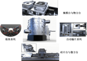
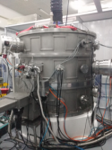
EUV technology testing platform from 2017, kinda like the concept. Looks suitable to test SSMB as a light source.

1663006883614.png1663006929930.png

Please, Log in or Register to view URLs content!

Please, Log in or Register to view URLs content!

General Research Laboratory of Microelectronics Equipment of the Institute of Optoelectronics has made breakthroughs in key unit technologies such as vacuum, film transport, workpiece table, vibration reduction and focus detection: the vacuum system achieves a stable high vacuum environment of 5.8 × 10 -7 Torr , ensuring that The stability of EUV light source propagation is improved; the frame and vibration reduction system of the whole machine meet the VC-F vibration reduction standard, and the vibration isolation effect is good in the frequency range of 2.2Hz - 500Hz in the horizontal direction and 2Hz- 500Hz in the vertical direction . The frame, workpiece table and mask table The stability meets the requirements of 32nm lithography and sub-nanometer wave aberration detection; the leveling and focusing detection system achieves nanometer-level detection accuracy, which provides a guarantee for the continuous multiple repetition of 32nm lithography resolution. At the same time, in the development of the workpiece table, the collaborative control technology of multiple workpiece tables is studied on the basis of the existing ones, which solves the problems of simultaneous control and position switching of the wafer table and the image table, the mask table and the object table; the automatic film feeding system Realize automatic loading and unloading in a vacuum environment ; the software system completes multi-module complex control, and coordinates each sub-system to complete the exposure process.

On the basis of completing the development of the key unit system, it has played a great role in cooperating with the overall project unit Changchun Institute of Optics and Mechanics to achieve 32nm repeatable exposure and with Shanghai Institute of Optics and Mechanics to achieve sub-nanometer wave aberration detection, which has been greatly affected by the overall project unit and each subject unit. And the acceptance group experts praised. During the research and development of the subject, the research group has achieved a series of original achievements in the fields of workpiece table control and precision measurement technology, and has applied for 31 invention patents , including 28 domestic patents and 3 international patents .
 

GodRektsNoobs

Junior Member
Registered Member
As I said in the beginning, this story was Western propaganda on the part of sanctions hawks who wanted political capital to push the CHIPS Act, so they released it right before the bill was going to a final vote. There were some people saying CHIPS was a violation of free trade and China was so far behind there was no need for industrial policy. The WSJ was giving voice to these folks because it's still a throwback to the last dying vestiges of Reagan capitalism.

Never trust a report by that D. Patel guy's firm.
LMAO. Did you even read the post? So something that is eqivalent of 1st gen TSMC 7nm is hopelessly behind? They admitted that it's similar to Intel 10nm+, and this is just N+1. There is no doubt at this point N+2 will at least be "true" 7nm even by their standard, if not better. Just for everyday reference, Qualcomm Snapdragon 855 is made using 1st generation TSMC 7nm process, and its upgraded variant Snapdragon 860 is still considered a quasi-flagship chip used on flagship killer phones.
 
Last edited:

GodRektsNoobs

Junior Member
Registered Member
EUV technology testing platform from 2017, kinda like the concept. Looks suitable to test SSMB as a light source.

View attachment 97418View attachment 97419

Please, Log in or Register to view URLs content!

Please, Log in or Register to view URLs content!

General Research Laboratory of Microelectronics Equipment of the Institute of Optoelectronics has made breakthroughs in key unit technologies such as vacuum, film transport, workpiece table, vibration reduction and focus detection: the vacuum system achieves a stable high vacuum environment of 5.8 × 10 -7 Torr , ensuring that The stability of EUV light source propagation is improved; the frame and vibration reduction system of the whole machine meet the VC-F vibration reduction standard, and the vibration isolation effect is good in the frequency range of 2.2Hz - 500Hz in the horizontal direction and 2Hz- 500Hz in the vertical direction . The frame, workpiece table and mask table The stability meets the requirements of 32nm lithography and sub-nanometer wave aberration detection; the leveling and focusing detection system achieves nanometer-level detection accuracy, which provides a guarantee for the continuous multiple repetition of 32nm lithography resolution. At the same time, in the development of the workpiece table, the collaborative control technology of multiple workpiece tables is studied on the basis of the existing ones, which solves the problems of simultaneous control and position switching of the wafer table and the image table, the mask table and the object table; the automatic film feeding system Realize automatic loading and unloading in a vacuum environment ; the software system completes multi-module complex control, and coordinates each sub-system to complete the exposure process.

On the basis of completing the development of the key unit system, it has played a great role in cooperating with the overall project unit Changchun Institute of Optics and Mechanics to achieve 32nm repeatable exposure and with Shanghai Institute of Optics and Mechanics to achieve sub-nanometer wave aberration detection, which has been greatly affected by the overall project unit and each subject unit. And the acceptance group experts praised. During the research and development of the subject, the research group has achieved a series of original achievements in the fields of workpiece table control and precision measurement technology, and has applied for 31 invention patents , including 28 domestic patents and 3 international patents .
Wow, that is impressive. It sounds like by 2017 CIOMP had something that was superior to ASML Alpha Demo Tool of 2006, although Alpha Demo Tool did manage to achieve 32nm exposure after upgrades. Seems that a NXE:3100 equivalent by 2023 will not only be likely, but actually be overdue since it only took ASML 4 years to reach that stage. Prof. Hiroo Kinoshita first proposed EUV lithography in 1985, and by 2017 China managed to close the technological gap from over 2 decades to around a single decade. At this point, it's honestly understandable that technological sanctions are absolutely necessary from the standpoint of US. Nevertheless, NXE:3100 is nowhere near volume production of 7/5nm chips. It remains to be seen when China will possess NXE:3400B equivalent.

Please, Log in or Register to view URLs content!
 

FairAndUnbiased

Brigadier
Registered Member
You are correct, but they have hold almost the same exact vacuum environment for an extended period that require a lot of sensing technology to detect leaks and others issues related to vacuum environments.
Out of curiosity I looked up what pumps ASML uses. They separate the EUV chamber into 2 regions:

Wafer chamber: Large diameter maglev turbos can usually run at slower RPM and worse base pressure (still 1E-8 mbar baseline though) than small turbos but are good for throughput and corrosion resistance.

EUV source chamber: Very high throughput screw pumps to handle hydrogen flow.

Please, Log in or Register to view URLs content!

Now I'm curious about whether they exclude hydrogen from the wafer chamber with differential pumping, a window, or they just let conduction bottleneck + high pump speed do the rest.

Here's a Chinese company offering the same.

Please, Log in or Register to view URLs content!

They have both maglev turbos and dry screw pumps.
 

AndrewS

Brigadier
Registered Member
You do realize that China won't be adding just mega fabs right?

Of course

They have over 30 fabs under construction and only 3 are 100k wpm 12-inch foundries. I'd have to look around for some data sources to see how many under construction are 8-inch and how many are 12-inch and the capacities for them. It seems to me that only SMIC has the resources right now to build 100k wpm megafabs. They are building 3 and only have 1 in operation. Everyone else is just building like 30k here and then expand 30k later and so forth. Also, we are about to hit a major global recession.

But if they have 20 8-inch fabs of average 50k wpm + another 12 12-inch fabs of average 40k wpm under construction -> that would be about 2.2 million 8-inch wpm. That's quite a bit of capacity coming online every 2 years. With an impending global recession, demand is also not going to grow at same rate as the last couple of years.

Are you sure this capacity is coming online in 2 years? It doesn't match up with the data below.

For 2022, Taiwan+Korea are expected to account for $59 Bn (54% of global fab investment)
In comparison, China is only at $17 Billion (16% of global fab investment)

Please, Log in or Register to view URLs content!

---

30 Chinese Fabs in 2 years also also doesn't match up with the reported sales of DUV systems from ASML to China in 2021, nor the anticipated fab starts below

Please, Log in or Register to view URLs content!
 

tphuang

Lieutenant General
Staff member
Super Moderator
VIP Professional
Registered Member
Of course


Are you sure this capacity is coming online in 2 years? It doesn't match up with the data below.

For 2022, Taiwan+Korea are expected to account for $59 Bn (54% of global fab investment)
In comparison, China is only at $17 Billion (16% of global fab investment)

Please, Log in or Register to view URLs content!

---

30 Chinese Fabs in 2 years also also doesn't match up with the reported sales of DUV systems from ASML to China in 2021, nor the anticipated fab starts below

Please, Log in or Register to view URLs content!
wsj is the one that said China has 31 "major semiconductor factories"
Please, Log in or Register to view URLs content!


Some of that will take 3 years like the 100 wpm mega fab from SMIC in Beijing and Shanghai. Keep in mind they are also trying to put new domestic equipments in them, so that would take longer to bring online. But most of the fabs seem to take a year or two to build. Like the one that BYD put online recently.
Please, Log in or Register to view URLs content!
or the one that SMIC is building in Shenzhen. It was announced in Mar 2021 and is supposed to go into production this year.

On top of that, there is also expansion on existing fabs like the Cansemi 12 inch fab and the Huahong Wuxi fab. I'm not sure those are counted in the 31 major semiconductor factories. It's far more likely for Chinese chipmakers (outside) to add capacity in smaller increments rather than 100k wpm at a time since they don't have the same funding as TSMC and Samsung.

I'm not sure why China needs ASML DUVs for most of these 8 inch fabs that are of more mature nodes. I don't know the exact number they are importing this year from ASML, but it sounded like a lot from their Q1 numbers and other rumors on this forum. Also, second hand ASML DUVs are probably sufficient for everything outside of SMIC's advance node foundry.
 

gelgoog

Lieutenant General
Registered Member
I'm not sure why China needs ASML DUVs for most of these 8 inch fabs that are of more mature nodes. I don't know the exact number they are importing this year from ASML, but it sounded like a lot from their Q1 numbers and other rumors on this forum. Also, second hand ASML DUVs are probably sufficient for everything outside of SMIC's advance node foundry.
What second hand? All world fab capacity is being used just about. The chip market is supposed to go into oversupply this year though.
 

tokenanalyst

Brigadier
Registered Member
CETC has funded yet another research institute for development semiconductor related technologies.

On September 7, China Electric Power Industry Basic Research Institute and Chip Technology Research Institute were inaugurated in Beijing. Hebei Semiconductor Research Institute (the 13th China Electric Power Research Institute) officially changed its name to the China Electric Power Industry Basic Research Institute (the 13 China Electric Power Research Institute). Chen Zhaoxiong, Secretary of the Party Group and Chairman of CETC, Zhang Chaochao, Member of the Standing Committee of the Hebei Provincial Party Committee and Secretary of the Shijiazhuang Municipal Party Committee, and Xiong Xue, Deputy Mayor of Chongqing and Secretary of the Party Working Committee of Chongqing High-tech Zone of Western Science City, attended the ceremony and delivered speeches. Li Shouwu, deputy secretary of the party group and director of CETC, presided over the meeting, and He Song, deputy general manager, read out the approval documents of relevant central departments and group companies.

Chen Zhaoxiong said that the establishment of the Industrial Basic Research Institute and the Chip Technology Research Institute is an important measure for CETC to thoroughly study and implement the spirit of General Secretary Xi Jinping's important speech and important instructions, promote the research on integrated circuits and core components, and accelerate breakthroughs in key core technologies. The establishment of the research institute will be the new starting point, aiming at the urgent and long-term needs of the country, systematically integrating the superior resources of integrated circuits and core components, making every effort to advance the industrial foundation and modernizing the industrial chain, and strive to become a world-class scientific research institute. Take the lead in making breakthroughs in construction, and make new and greater contributions to accelerating the realization of high-level scientific and technological self-reliance in the field of electronic information.

Zhang Chaochao said that the establishment of the China Electric Power Industry Basic Research Institute is a vivid practice of in-depth study and implementation of General Secretary Xi Jinping's important statement on achieving high-level scientific and technological self-reliance and self-reliance, and a practical action to vigorously implement the innovation-driven development strategy, which will definitely promote the electronics industry. The acceleration of the innovation chain to achieve new breakthroughs will also inject strong impetus into the economic development of Shijiazhuang. It is hoped that the two sides will continue to strengthen practical cooperation, and take the establishment of the Industrial Basic Research Institute as an opportunity to promote more high-quality enterprises and projects to settle in Shijiazhuang, and strive to build a model of mutually beneficial and win-win development between central enterprises and local governments.

Xiong Xue said that CETC has established a chip technology research institute based on its advantageous resources to carry out key and core chip technology research, which reflects the enterprising consciousness of keeping pace with the times, the responsibility of serving technology for self-reliance and self-improvement, and the pragmatic attitude of maintaining the safety and stability of the industrial chain. It is hoped that the Institute of Chip Technology will speed up the construction of a first-class platform, introduce a first-class team, make breakthroughs in first-class technology, and produce first-class results, so as to effectively enhance the source function of scientific and technological innovation in the field of integrated circuits and the industrialization ability of scientific and technological achievements, and help Chongqing to build a "smart city" and build "Smart City".

1663013840230.png
 
Status
Not open for further replies.
Top