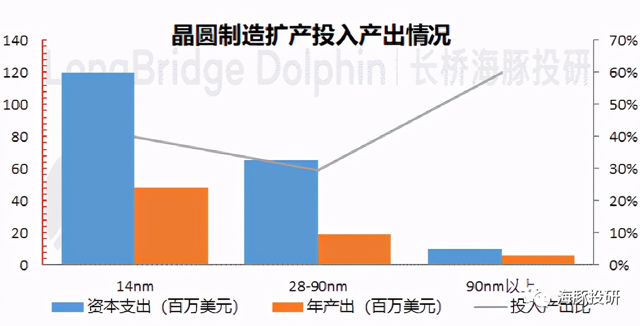
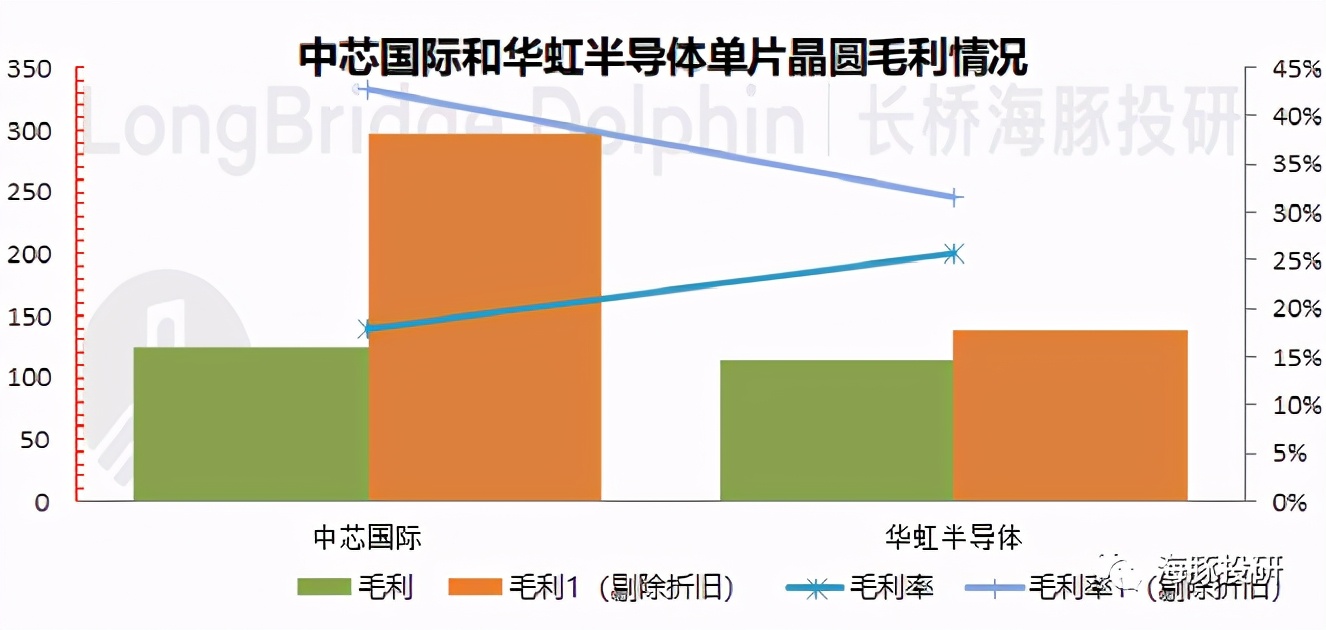
Bro a brief history regarding SMIC expansion plan and growth strategy.
In 2020, SMIC will take advantage of the sci-tech innovation board to return to the big A listing. As the most well-known wafer manufacturing company in mainland China, SMIC has leading production capacity and process capability. While carrying the expectations and vision of the semiconductor industry, it also puts the company at the forefront of Sino-US technological friction.
In recent years, "China-US frictions" and "US sanctions" have frequently appeared in the public eye, and Huawei and SMIC are in the front line.
First, Huawei. On May 15, 2020, the U.S. Department of Commerce conducted licensing controls on the supply of Huawei chips; then on August 17, the purchase of Huawei chips was restricted, and it became effective on September 15.
For SMIC, the Trump administration added it to the list of entities, specifically restricting the purchase of equipment required for advanced processes of 10nm and below; the Biden administration signed an executive order to continue the identification of SMIC restricted entities.
After several rounds of international competitions, SMIC's performance has been significantly damaged, which has suppressed the performance of the capital market. For example, in terms of performance, Huawei was previously a major customer of the company and contributed more than 20% of SMIC's revenue.
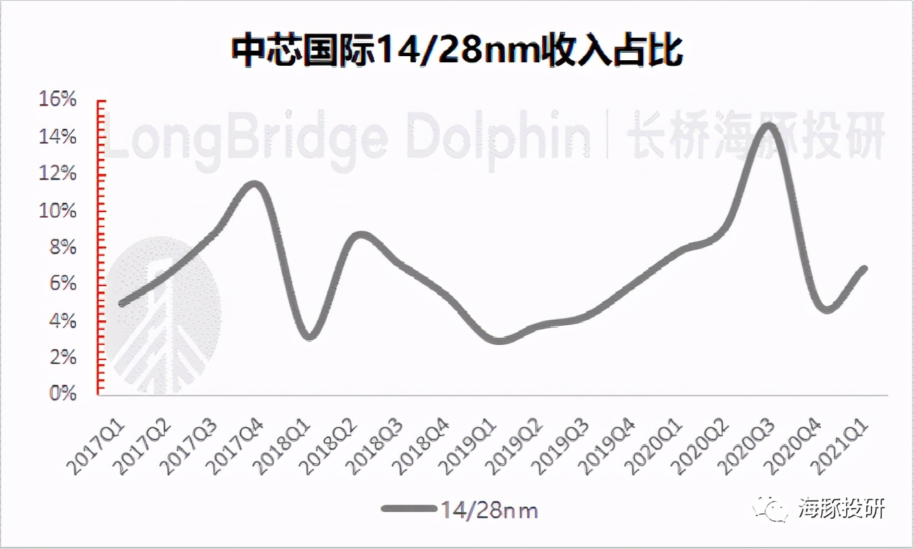
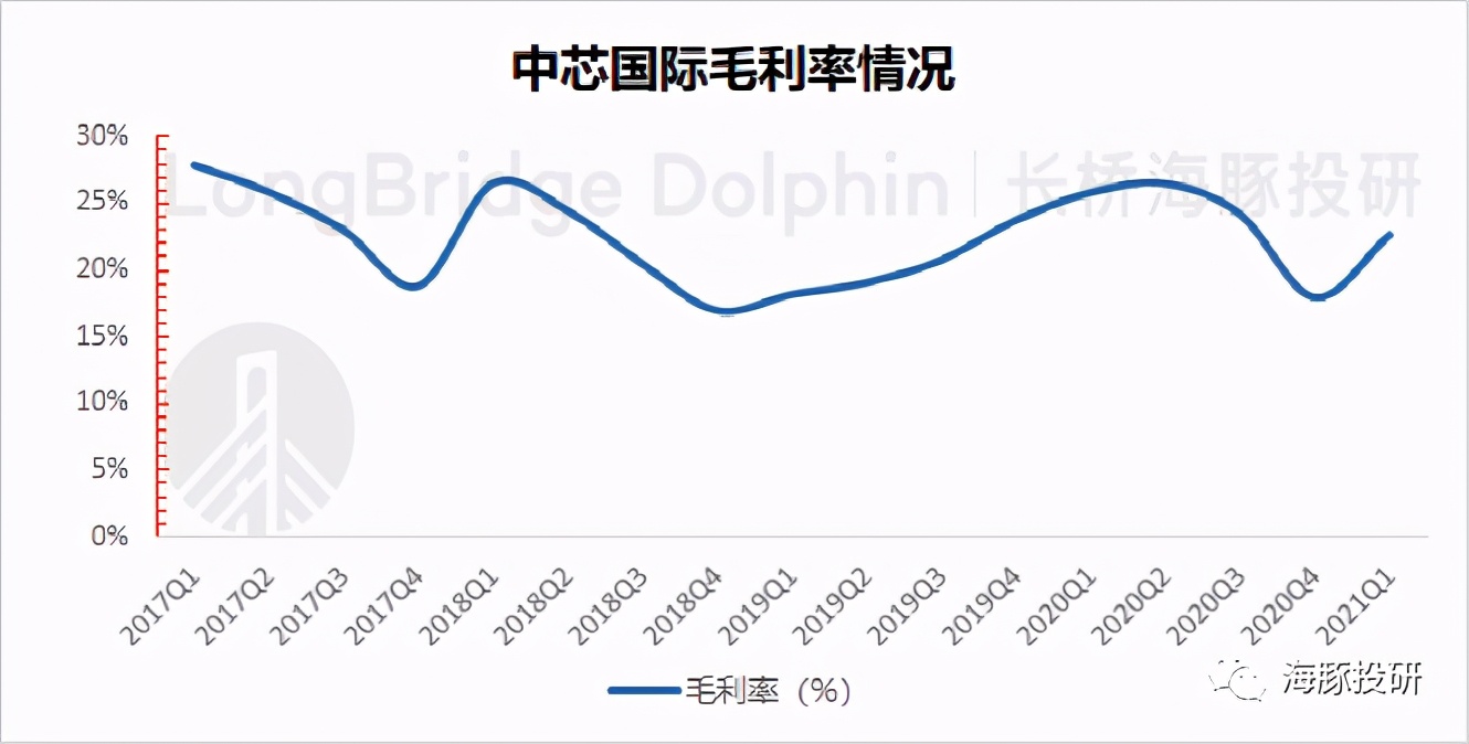
With the entry into force of Huawei's restriction order in mid-September last year, Huawei rushed to substantially increase its purchases before the effective date. Corresponding to SMIC's performance, the company's 14/28nm (Huawei's main procurement process segment) revenue accounted for a significant increase in the third quarter, and then severely declined in the following quarter, and gross profit margin also experienced a significant decline in Q4.
Affected by the US entity list, SMIC's customers and production capacity structure have been adjusted.
In terms of capital market trends, SMIC is strongly related to sanctions and international relations expectations (see below). In June of this year, Biden continued his predecessor's policy with certainty and implemented double-list restrictions on SMIC. , SMIC did not reflect the upward flexibility that its domestic counterparts should have, and its overall performance continued to be sluggish.
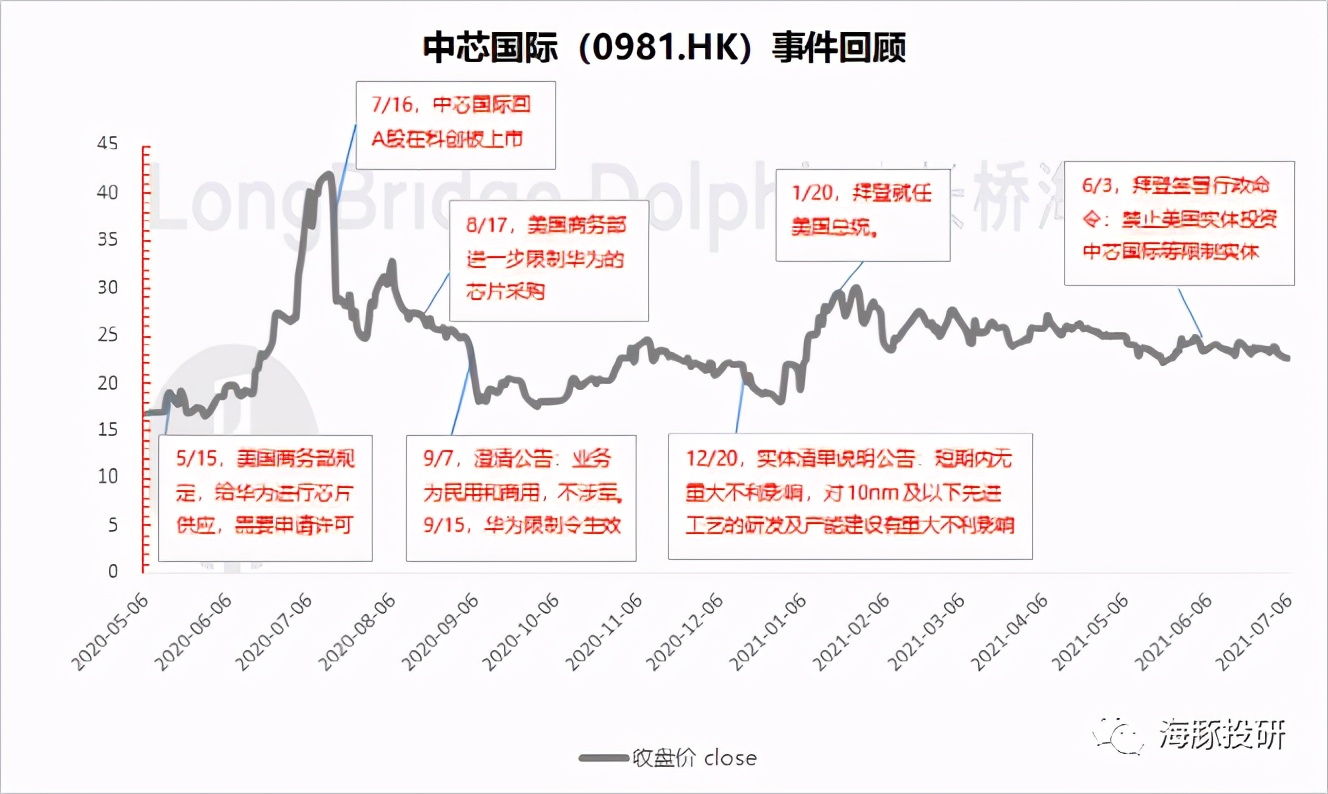
As for Dolphin's series of researches on SMIC, he hopes to try to understand that SMIC will continue to "lie on his stomach" through analysis of the industry situation, SMIC's position and competitive outlook, and there is still a chance for reversal.
In order to answer this question, Mr. Dolphin is mainly concerned with the following questions:
1) After 20 years, in terms of process technology, it has laid out 14nm-0.35um node process;
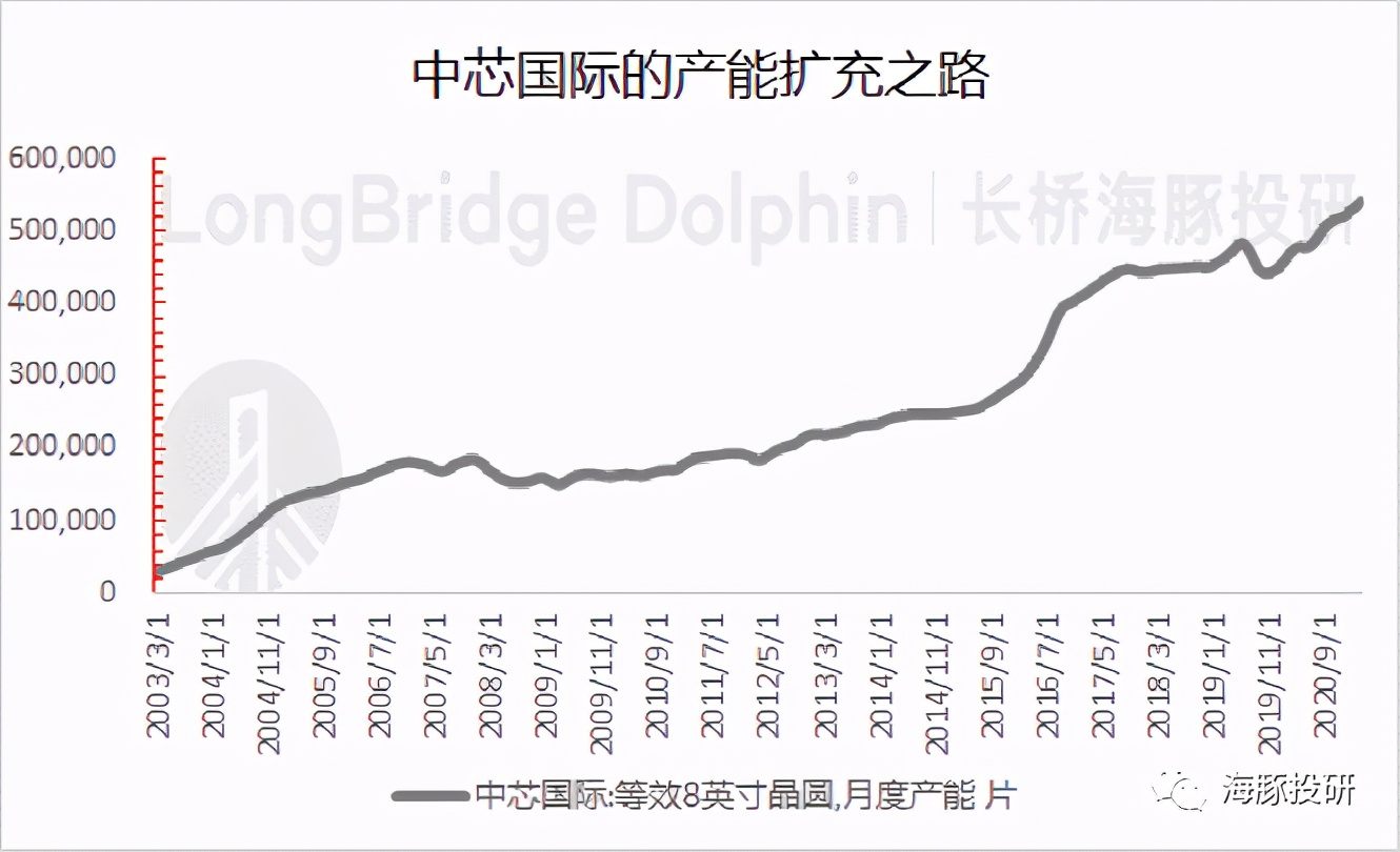
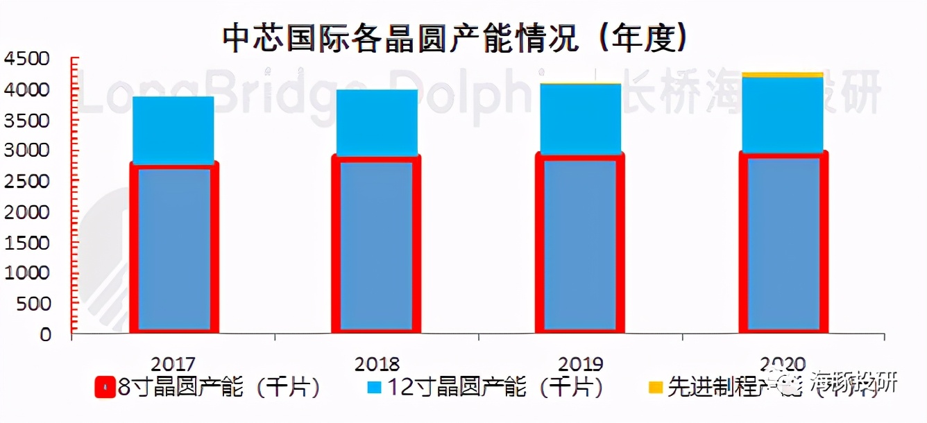
2) Three 8-inch wafer fabs and four 12-inch wafer fabs have been built in terms of production capacity. Among them, the 8-inch production capacity totals about 270,000 pieces/month, the 12-inch production capacity totals about 118,000 pieces/month, and the total production capacity exceeds 540,000 pieces/month (equivalent to 8 inches).
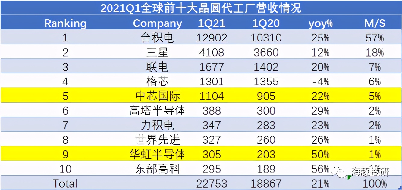
3) In the global wafer foundry revenue of 2021Q1, SMIC achieved US$1.104 billion, ranking No. 5 in the world and No. 1 in Mainland China.
As a whole, whether it is the layout of nodes, the volume of production capacity or the scale of income generation, it is a well-deserved domestic industry brother.
In terms of specific revenue composition: SMIC's core is the wafer business, with additional wafer-related mask manufacturing & wafer testing and other revenue components.
The wafer business covers 8-inch wafer production lines, 12-inch wafer production lines and advanced process wafer production lines. Mask manufacturing, wafer testing and other revenues cover design services and IP support, photomask manufacturing, and bump processing and testing.
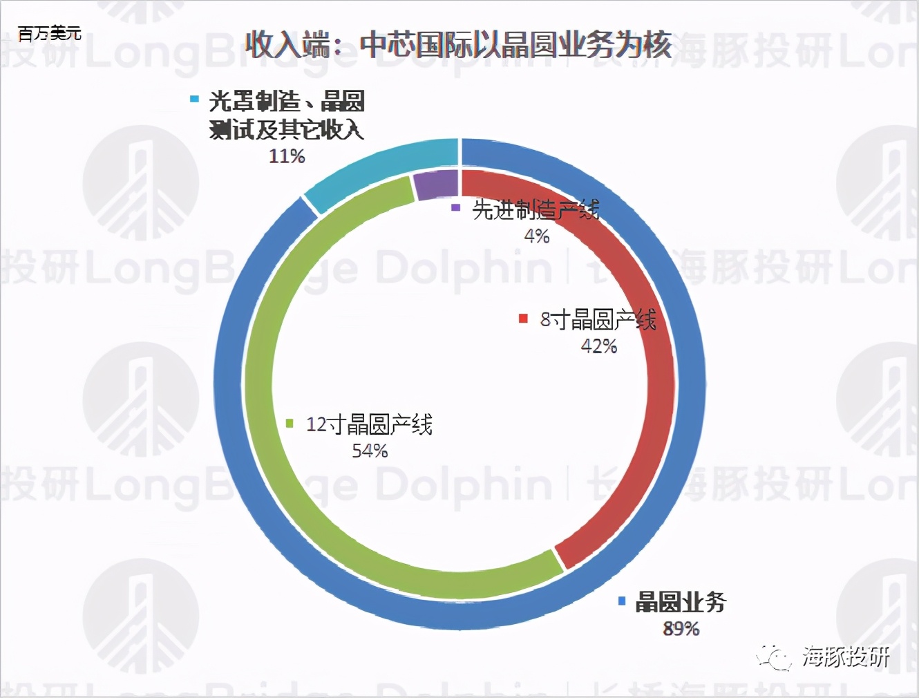
In the current business structure, the wafer business accounts for around 90%, and the revenue from photomask manufacturing, wafer testing and other revenues account for a relatively small proportion.
In the wafer business segmented by size, although 8-inch wafers accounted for more than 40% of their revenues, although they declined, 12-inch wafers benefited from the advancement of domestic customer cooperation, accounting for 54%; advanced process end realization A breakthrough in mass production.
1) 8-inch wafer production lines mainly include Shanghai Fab S1, Tianjin Fab7 and Shenzhen Fab15 production lines, and their products are mainly oriented to 0.11/0.13um, 0.15/0.18um and 0.25um/0.35um.
The application areas of 8-inch wafers mainly include power devices (usually used in automotive and industrial applications), analog ICs such as PMIC and LED drivers, smart card chips and other fields;
2) The 12-inch wafer production lines mainly include Shanghai Fab S2, Beijing Fab B1, Shenzhen Fab16 and SMIC Fab B2 and B3. The products are mainly for 90nm and below process processes.
12-inch wafers are mainly applicable to radio frequency ICs such as Nor Flash, CIS, WiFi Bluetooth chips, set-top box chips, and wearable APs;
3) Advanced process production lines are mainly deployed in SMIC South, mainly for process nodes of 14nm and below. The main application areas of advanced process wafer products are GPU, FPGA, mining machine ASIC, flat AP and other fields.
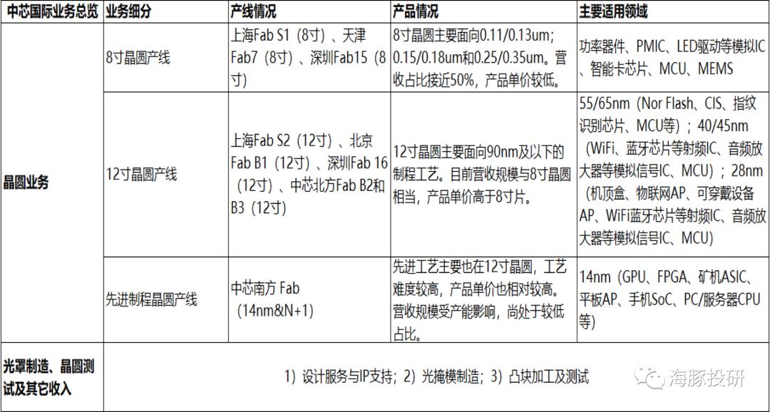
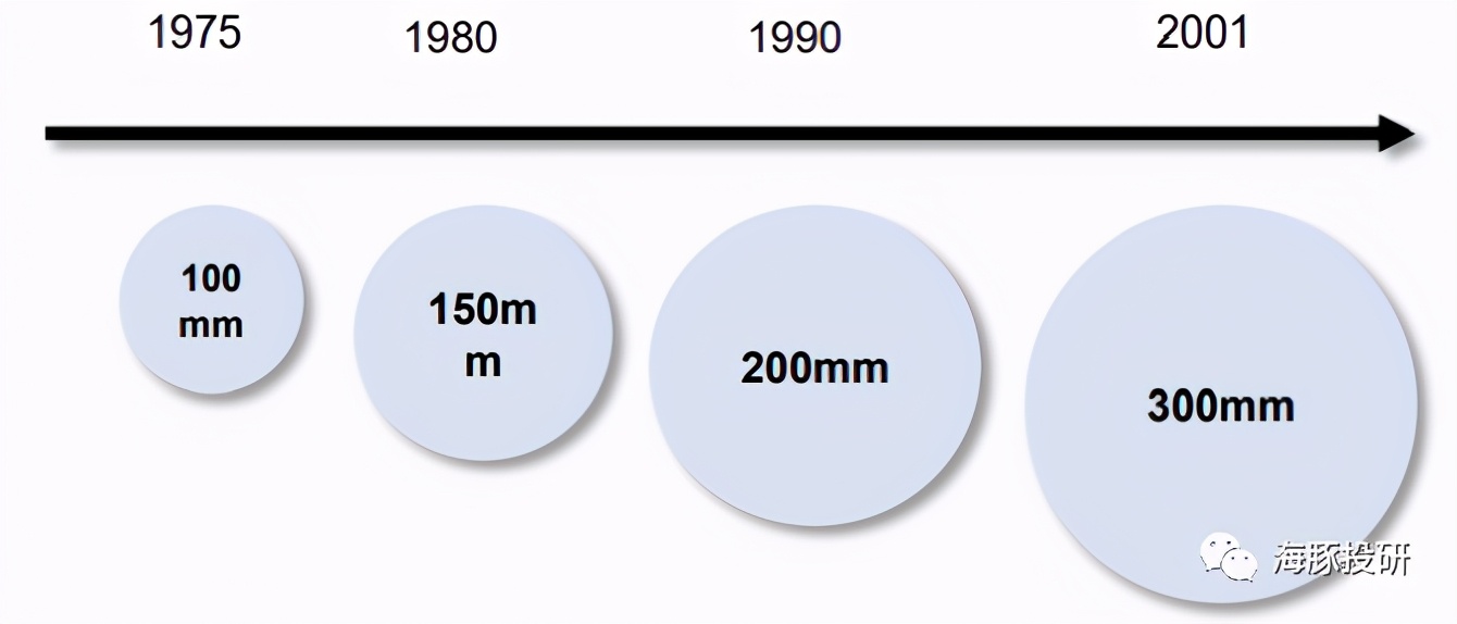
Many people may still find it difficult to understand the meaning behind the above industrial layout. Dolphin here introduces the evolution path of wafer size.
From the perspective of product evolution path, under the influence of Moore's Law, the integration of integrated circuits will only go on the road. The main ways to improve the integration of integrated circuits are to increase the chip area, reduce the feature size of the device, and improve the circuit and structural design.
1) Increasing the chip area: The continuous increase in the diameter of silicon wafers used in the production of circuits has led to a substantial increase in production efficiency. The diameter of mainstream silicon wafers has reached 12 inches;
2) Reduce the feature size of the device: the processing accuracy, the degree of automation and the reliability are improved.
3) The expansion of wafer size improves production efficiency: Due to the unevenness and defects on the periphery of the silicon wafer, the middle part of the wafer is mainly used. The diameter of the silicon wafer ranges from 200mm (8-inch wafer) to 300mm (12-inch). The available area on the silicon wafer is larger, and the more chips can be produced on a wafer, the efficiency can be improved and the cost can be reduced.
SMIC: On the "core" technology of the leader
2022-09-09 16:46 HKTIn 2020, SMIC will take advantage of the sci-tech innovation board to return to the big A listing. As the most well-known wafer manufacturing company in mainland China, SMIC has leading production capacity and process capability. While carrying the expectations and vision of the semiconductor industry, it also puts the company at the forefront of Sino-US technological friction.
In recent years, "China-US frictions" and "US sanctions" have frequently appeared in the public eye, and Huawei and SMIC are in the front line.
First, Huawei. On May 15, 2020, the U.S. Department of Commerce conducted licensing controls on the supply of Huawei chips; then on August 17, the purchase of Huawei chips was restricted, and it became effective on September 15.
For SMIC, the Trump administration added it to the list of entities, specifically restricting the purchase of equipment required for advanced processes of 10nm and below; the Biden administration signed an executive order to continue the identification of SMIC restricted entities.
After several rounds of international competitions, SMIC's performance has been significantly damaged, which has suppressed the performance of the capital market. For example, in terms of performance, Huawei was previously a major customer of the company and contributed more than 20% of SMIC's revenue.
With the entry into force of Huawei's restriction order in mid-September last year, Huawei rushed to substantially increase its purchases before the effective date. Corresponding to SMIC's performance, the company's 14/28nm (Huawei's main procurement process segment) revenue accounted for a significant increase in the third quarter, and then severely declined in the following quarter, and gross profit margin also experienced a significant decline in Q4.
Affected by the US entity list, SMIC's customers and production capacity structure have been adjusted.


In terms of capital market trends, SMIC is strongly related to sanctions and international relations expectations (see below). In June of this year, Biden continued his predecessor's policy with certainty and implemented double-list restrictions on SMIC. , SMIC did not reflect the upward flexibility that its domestic counterparts should have, and its overall performance continued to be sluggish.

As for Dolphin's series of researches on SMIC, he hopes to try to understand that SMIC will continue to "lie on his stomach" through analysis of the industry situation, SMIC's position and competitive outlook, and there is still a chance for reversal.
In order to answer this question, Mr. Dolphin is mainly concerned with the following questions:
- Where is SMIC's competitive advantage?
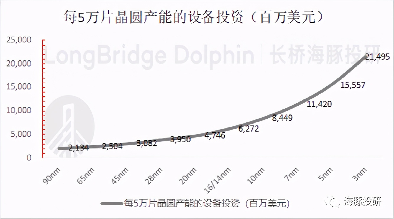
- How much is the input and output of wafer manufacturing expansion?
- How to judge the investment value and valuation of SMIC?
, SMIC: SMIC's fire is gradually gaining momentum
SMIC was founded in adversity, from the mass production of the first 8-inch line in 2002 to the first 12-inch line in 2005, and then to the current production of multiple 8-inch/12-inch wafers in Shanghai, Shenzhen, and Beijing. line.1) After 20 years, in terms of process technology, it has laid out 14nm-0.35um node process;
2) Three 8-inch wafer fabs and four 12-inch wafer fabs have been built in terms of production capacity. Among them, the 8-inch production capacity totals about 270,000 pieces/month, the 12-inch production capacity totals about 118,000 pieces/month, and the total production capacity exceeds 540,000 pieces/month (equivalent to 8 inches).
3) In the global wafer foundry revenue of 2021Q1, SMIC achieved US$1.104 billion, ranking No. 5 in the world and No. 1 in Mainland China.
As a whole, whether it is the layout of nodes, the volume of production capacity or the scale of income generation, it is a well-deserved domestic industry brother.
In terms of specific revenue composition: SMIC's core is the wafer business, with additional wafer-related mask manufacturing & wafer testing and other revenue components.
The wafer business covers 8-inch wafer production lines, 12-inch wafer production lines and advanced process wafer production lines. Mask manufacturing, wafer testing and other revenues cover design services and IP support, photomask manufacturing, and bump processing and testing.

In the current business structure, the wafer business accounts for around 90%, and the revenue from photomask manufacturing, wafer testing and other revenues account for a relatively small proportion.
In the wafer business segmented by size, although 8-inch wafers accounted for more than 40% of their revenues, although they declined, 12-inch wafers benefited from the advancement of domestic customer cooperation, accounting for 54%; advanced process end realization A breakthrough in mass production.
1) 8-inch wafer production lines mainly include Shanghai Fab S1, Tianjin Fab7 and Shenzhen Fab15 production lines, and their products are mainly oriented to 0.11/0.13um, 0.15/0.18um and 0.25um/0.35um.
The application areas of 8-inch wafers mainly include power devices (usually used in automotive and industrial applications), analog ICs such as PMIC and LED drivers, smart card chips and other fields;
2) The 12-inch wafer production lines mainly include Shanghai Fab S2, Beijing Fab B1, Shenzhen Fab16 and SMIC Fab B2 and B3. The products are mainly for 90nm and below process processes.
12-inch wafers are mainly applicable to radio frequency ICs such as Nor Flash, CIS, WiFi Bluetooth chips, set-top box chips, and wearable APs;
3) Advanced process production lines are mainly deployed in SMIC South, mainly for process nodes of 14nm and below. The main application areas of advanced process wafer products are GPU, FPGA, mining machine ASIC, flat AP and other fields.

Many people may still find it difficult to understand the meaning behind the above industrial layout. Dolphin here introduces the evolution path of wafer size.
From the perspective of product evolution path, under the influence of Moore's Law, the integration of integrated circuits will only go on the road. The main ways to improve the integration of integrated circuits are to increase the chip area, reduce the feature size of the device, and improve the circuit and structural design.
1) Increasing the chip area: The continuous increase in the diameter of silicon wafers used in the production of circuits has led to a substantial increase in production efficiency. The diameter of mainstream silicon wafers has reached 12 inches;
2) Reduce the feature size of the device: the processing accuracy, the degree of automation and the reliability are improved.
3) The expansion of wafer size improves production efficiency: Due to the unevenness and defects on the periphery of the silicon wafer, the middle part of the wafer is mainly used. The diameter of the silicon wafer ranges from 200mm (8-inch wafer) to 300mm (12-inch). The available area on the silicon wafer is larger, and the more chips can be produced on a wafer, the efficiency can be improved and the cost can be reduced.
Last edited:

