Xtacking 3.0 officially debuted YMTC once again broke through the technical barrier
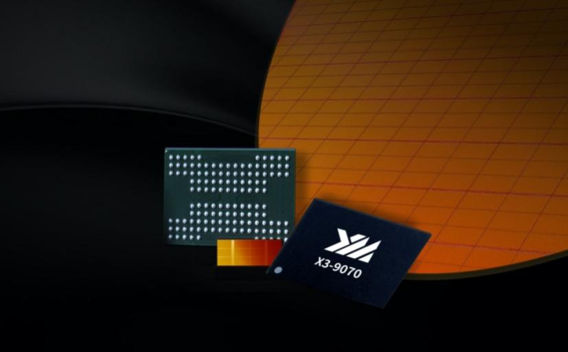
At the 2022 Flash Memory Summit, the annual event of storage technology, Yangtze Memory Technologies Co., Ltd. (YMTC) officially released its heavyweight product, the fourth-generation TLC 3D flash memory X3-9070 based on Xtacking® 3.0 (Xtacking® 3.0) technology.
2400MT/s I/O transfer rate, 1Tb capacity in a smaller single chip, 50% increase in performance and 25% reduction in power consumption, the key indicators of X3-9070 have reached the top level in the industry. At the same time, the launch of the third-generation Xtacking technology has also enabled YMTC to have greater initiative in the increasingly fierce competition in storage technology.
Crystal stack technology upgrade
Xtacking technology is the core of the strong competitiveness of YMTC's flash memory series. Since its introduction in 2018, this technology has brought higher density, faster I/O speeds and shorter time-to-market to flash products.
Xtacking technology places peripheral circuits on top of memory cells, allowing chip processing to move from plane to three-dimensional. That is, peripheral circuits are processed on one wafer, memory cells are processed on another wafer, and the two wafers are respectively completed and then bonded through millions of metal VIAs (Vertical Interconnect Accesses, vertical interconnection channels). Compared with traditional 3D NAND flash memory architecture, Xtacking can bring faster I/O transfer speed, higher storage density and shorter time to market.
Xtacking technology has four advantages: first, better performance, second, more advanced technology, third, cost advantages, and fourth, higher flexibility.
In traditional 3D NAND flash memory, the area occupied by peripheral chips is about 30-40%. As the number of stack layers increases to more than 128 layers, the area occupied by peripheral chips will reach more than 50%. The Xtacking structure reduces the area of peripheral chips. A higher density than conventional NAND flash memory is achieved.
At the same time, Xtacking realizes parallel and modular product design and manufacturing, which can shorten the product development time by three months and shorten the production cycle by 20%, thereby greatly shortening the time-to-market of 3D NAND products. In addition, this modular approach also makes it possible to introduce innovative functions of NAND peripheral circuits to realize the customization of NAND flash memory.
X3-9070 adopts the latest
Xtacking 3.0 architecture. After years of iterative innovation, the latest Xtacking technology has made the X3-9070 the highest density flash memory particle product in the history of YMTC, achieving a storage capacity of 1Tb with a smaller chip size.
For the performance of Xtacking technology, Gregory Wong, founder and chief analyst of Forward Insights, gave a very high evaluation, believing that the hybrid bonding technology of storage array and peripheral logic circuit is very important to promote the innovative development of 3D NAND technology.
Gregory Wong emphasized: "The X3-9070 is a key industry milestone equipped with the advanced flash memory technology chip stack 3.0 platform. This also indicates that the hybrid bonding technology of memory cells and peripheral logic circuits is expected to become the mainstream of the industry in the future."
After the iterative development of Xtacking from 1.0 to 3.0, YMTC has accumulated rich experience in the field of 3D heterogeneous integration, and has successfully built a number of YMTC storage system solution products based on crystal stack technology, including SATA III, PCIe Gen3, Gen4 Solid-state drives, as well as embedded storage products such as eMMC and UFS for mobile communications and other embedded applications, have won wide acclaim from industry partners.
Realize 200+ layer stack and constantly break the limit
The competition of storage technologies, on the one hand, is the reading speed, and on the other hand, the storage density. When flash memory enters the 3D era, stacking technology is mainly used to achieve larger storage capacity in a smaller space and area. Therefore, the number of stacked layers replaces the process and becomes the new flash memory evaluation standard. As leading companies continue to expand the market layout of 3D NAND flash memory and promote technological innovation and evolution, the stack height of 3D NAND flash memory is constantly breaking the limit.
Although it started late, YMTC dared to innovate in technology. It started from 32-layer stack, and after the accumulation of 64-layer stack, it skipped the 96-layer stack flash memory promoted by Samsung, Micron, Toshiba and other companies, and carried out 128-layer 3D NAND. The research and development of flash memory, and the success of the research and development will be officially announced in 2020.
The 128-layer 3D NAND flash memory produced by YMTC has the highest storage density per unit area, the highest I/O transmission speed and the highest single NAND flash memory chip capacity among known models in the industry. In just three years, YMTC has achieved the leap from 32 to 128 floors.
After the breakthrough, YMTC's research and development speed continued to accelerate. Relevant media have reported that YMTC will skip the original 192-layer technology, directly challenge the higher number of layers, and mass-produce it by the end of 2022. Therefore,
the X3-9070 launched this time is full of expectations.
Although the official information on the number of stack layers of the X3-9070 has not been given, the product has reached the international leading technical level based on the characteristics of the product and the information provided by many industry insiders, which also marks another major breakthrough in domestic 3D NAND products. .
Breaking through the 200-layer mark can enable 3D NAND to obtain faster I/O speeds. Therefore, the X3-9070 achieves an I/O transfer rate of up to 2400MT/s, which is 50% more optimized than the previous generation.
Jiweiwang also noticed that the X3-9070 adopts a 6-plane design. You must know that by increasing the number of planes, the concurrency of the flash memory can be greatly improved, and the performance can be greatly improved. Therefore, compared with the traditional 4-plane, the performance of X3-9070 is improved by more than 50%, while the power consumption is reduced by 25%, which can bring more attractive total cost of ownership (TCO) to end users.
The more powerful performance also enables the X3-9070 to meet the needs of many emerging applications. As Chen Yi, Executive Vice President of YMTC said, "X3-9070 flash memory particles are YMTC's ingenious work in the field of 3D flash memory in recent years. It has excellent performance and extremely high storage density, and can be quickly and efficiently applied to mainstream applications. In commercial scenarios, we will face new demands and challenges brought about by the booming 5G, cloud computing, Internet of Things, autonomous driving, artificial intelligence and other new technologies.”