Chinese semiconductor industry

Status
Not open for further replies.

Blitzo

Lieutenant General
Staff member
Super Moderator
Registered Member
Well according to this website the 7nm is in production and thru tear down and reverse engineering of sample they determine
it is 7nm

Please, Log in or Register to view URLs content!

China’s SMIC Is Shipping 7nm Foundry ASICs​


Dylan Patel

2 hr ago


SMIC, China’s largest foundry has slowly been catching up to TSMC, Samsung, and various western foundries in process technology. They are rapidly approaching position as the world’s 3rd largest foundry and have higher margins than the current number 3, GlobalFoundries. SMIC has achieved this through a combination of large subsidies from the state, poaching TSMC talent, and tremendous home-grown expertise. Their chips ship in large volumes to a variety of use cases from smartphones to
Please, Log in or Register to view URLs content!
. The foundry has now quietly released and started mass production of their 7nm process node dubbed N+2.

We say quietly as this didn’t come directly from SMIC, but rather the reverse engineering and teardown firm TechInsights who purchased the chip on the open market and sent it to their labs. SMIC likely has not discussed this publicly on earnings reports as they are afraid of blowback. To be abundantly clear, China’s SMIC is shipping a foundry process with commercially available chips in the open market which are more advanced than any American or European company. While the US has high hopes for Intel to be the savior, there are no Intel 7nm class foundry chips commercially available for purchase currently and they still have to build out their foundry operations. The most advanced American or European foundry produced chips are based on GlobalFoundries 12nm.

SMIC’s 7nm just like TSMC’s 7nm and Intel’s 7nm class technologies does not use EUV lithography. TechInsights has more information in their 3 detailed reports titled “ASIC Digital Floorplan Analysis,” “(SMIC 7nm) Advanced CMOS Process Analysis,” and “(SMIC 7nm) Process Flow Analysis.” We recommend people check those out for more details.

This is a groundbreaking discovery because the US Department of Commerce was supposed to be restricting export licenses for any equipment which can be used on technologies more advanced than 14nm. Of course, the department of commerce handed out export licenses like candy as they always do. Furthermore, almost all equipment that is used on SMIC’s 14nm FinFET can be used on their 7nm process technology as well. While SMIC likely cannot develop beyond 7nm without EUV, they still should be able to ramp their 7nm over time to very large volumes. The US government is asleep at the wheel as Lam Research off-shores production and Intel uses subsidies to import equipment used to manufacturer chips from China. Government policy is why the US will lose semiconductors.

SMIC’s foundry customer, MinerVa states this chip has been in production since July of 2021. On September 22nd 2021, MinerVa’s website was updated with information about the product and the image above. It is a small 19.3mm2 chip used for mining cryptocurrencies, but in the future, this process technology could be scaled up and adopted for high end supercomputer and consumer applications. Their miner ships with 120 chips per board with 3 board per miner and a total power consumption of 3300W.

Just FYI, the above discussion was about the same article posted earlier on the last page.

 
Last edited:

Hendrik_2000

Lieutenant General
Just FYI, the aboce discussion was about the same article posted earlier on the last page.

But this article is different it tell us how they come to the conclusion that it was 7nm by tear down and RE and is in PRODUCTION! That is new

We say quietly as this didn’t come directly from SMIC, but rather the reverse engineering and teardown firm
Please, Log in or Register to view URLs content!
who purchased the chip on the open market and sent it to their labs. SMIC likely has not discussed this publicly on earnings reports as they are afraid of blowback. To be abundantly clear, China’s SMIC is shipping a foundry process with commercially available chips in the open market
 
Last edited:

wxw456

New Member
Registered Member
You may have a point but, I am a bit skeptical of these guys, specially in the context how they express themselves politically rather than technically.
Here are the claims being made:
  • TechInsights purchased a MinerVa Bitcoin Mining SoC fabbed by SMIC.
    • They performed a teardown and reverse engineering of the chip and concluded:
      • A 7nm process (N+2) was used to fab the chip.
      • It is comparable to TSMC 7nm.
    • Actual report is behind a paywall that I don't have access to:
  • The chip has been in production since July 2021.
  • It has been commercially available since September 2021 or earlier.
If this is true, then that means:
  • SMIC has made progress on its N+2 process since it was last confirmed in October 2020 that they taped out a chip made with their N+1 process.
  • We do not have an official confirmation if the N+2 process is in mass production (we may not get one even it does enter mass production). But we do know that commercial products have been made using the process.
  • Earlier there was talk of the US pressing ASML over a DUVL ban. Much of the discussion here was derailed and centered on the SMIC 28nm process.
    • Commentary
      Please, Log in or Register to view URLs content!
      assumed that it was targeted at the SMIC 14nm/12nm process. Furthermore they made the claim that SMIC N+1 and N+2 was cancelled or delayed.
      • This news contradicts the above commentary. It means that SMIC N+1 and N+2 are not cancelled and still progressing well.
    • It would also imply that the sanctions/restrictions applied by the US on SMIC was not capable of stopping development of SMIC's N+1 and N+2 process. ;)
      • Recall that the original goal of the sanctions was to stop SMIC at the 12nm/14nm node.
      • This might be why there was suddenly more news about additional semiconductor equipment sanctions/restrictions.
 

Blitzo

Lieutenant General
Staff member
Super Moderator
Registered Member
But this article is different it tell us how they come to the conclusion that it was 7nm by tear down and RE and is in PRODUCTION! That is new

No, the tweet in that post directly links to the same article that you did...

Thanks for posting the contents of the article here, but the discussions above is literally about the exact same article which was posted by @Wangxi.

Screenshot_20220721-134330~2.jpg
 

hvpc

Junior Member
Registered Member
it's just acceptance test, to develop photoresist and immersion device, it will officially launch in Q4 this year or Q1 next year...
Hi, @olalavn
What does "just acceptance test, to develop photoresist and immersion device" mean? Do you mean SMEE SSA800 will only used for acceptance testing of other equipment and to help with development of photoresist?

Any idea what the status of SMEE SSB800 & SSC800 is? thanks
 

tokenanalyst

Brigadier
Registered Member
Here are the claims being made:
  • TechInsights purchased a MinerVa Bitcoin Mining SoC fabbed by SMIC.
    • They performed a teardown and reverse engineering of the chip and concluded:
      • A 7nm process (N+2) was used to fab the chip.
      • It is comparable to TSMC 7nm.
    • Actual report is behind a paywall that I don't have access to:
  • The chip has been in production since July 2021.
  • It has been commercially available since September 2021 or earlier.
If this is true, then that means:
  • SMIC has made progress on its N+2 process since it was last confirmed in October 2020 that they taped out a chip made with their N+1 process.
  • We do not have an official confirmation if the N+2 process is in mass production (we may not get one even it does enter mass production). But we do know that commercial products have been made using the process.
  • Earlier there was talk of the US pressing ASML over a DUVL ban. Much of the discussion here was derailed and centered on the SMIC 28nm process.
    • Commentary
      Please, Log in or Register to view URLs content!
      assumed that it was targeted at the SMIC 14nm/12nm process. Furthermore they made the claim that SMIC N+1 and N+2 was cancelled or delayed.
      • This news contradicts the above commentary. It means that SMIC N+1 and N+2 are not cancelled and still progressing well.
    • It would also imply that the sanctions/restrictions applied by the US on SMIC was not capable of stopping development of SMIC's N+1 and N+2 process. ;)
      • Recall that the original goal of the sanctions was to stop SMIC at the 12nm/14nm node.
      • This might be why there was suddenly more news about additional semiconductor equipment sanctions/restrictions.
1658368191177.png

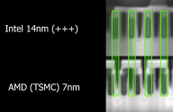
Intel 14nm vs TSMC 7nm very similar at plain view but different. That DOESN'T mean that SMIC 7m is not in RISK production but just looking to SEM images is difficult to tell.
 

latenlazy

Brigadier
Hi, @olalavn
What does "just acceptance test, to develop photoresist and immersion device" mean? Do you mean SMEE SSA800 will only used for acceptance testing of other equipment and to help with development of photoresist?

Any idea what the status of SMEE SSB800 & SSC800 is? thanks
I think he means that acceptance testing is the current phase the instrument is at in the instrument's adoption timeline. As in being accepted into use within a production workflow.
 

hvpc

Junior Member
Registered Member
But this article is different it tell us how they come to the conclusion that it was 7nm by tear down and RE and is in PRODUCTION! That is new

We say quietly as this didn’t come directly from SMIC, but rather the reverse engineering and teardown firm
Please, Log in or Register to view URLs content!
who purchased the chip on the open market and sent it to their labs. SMIC likely has not discussed this publicly on earnings reports as they are afraid of blowback. To be abundantly clear, China’s SMIC is shipping a foundry process with commercially available chips in the open market
These are sort of old news. SMIC announced N+1 capability almost 2years ago. N+1 is 7nm-like and for bitcoin mining application. Since these chips do not have SRAM on it and easier to produce at higher yield, can't be considered as true 7nm. My understanding is this is why SMIC called this 7nm-like as N+1 and true 7nm as N+2. N+1/N+2 SMIC had always seemed to imply these as 7nm-family of nodes. The industry consensus then refer to N+1 capability as 8nm to 10nm level.

All the brouhaha came about because TechInsight just now is able to obtain a physical chip to do a teardown analysis. But this chip, this SMIC capability is not new it's something SMIC is capable of at least a year or year and half ago.

People can call this chip 7nm, N+1, or 8nm/10nm depending on their perspectives or what definition they use, but I think all of these just refer to the same bitcoin mining chip. I don't know why people are surprised at something SMIC said they could do and produce long ago. The concept of western non-industry folks now have physical evidence so assume this is something 'new is just stupid. We had this awhile ago, this is yesterday's accomplishment.
 

Blitzo

Lieutenant General
Staff member
Super Moderator
Registered Member
These are sort of old news. SMIC announced N+1 capability almost 2years ago. N+1 is 7nm-like and for bitcoin mining application. Since these chips do not have SRAM on it and easier to produce at higher yield, can't be considered as true 7nm. My understanding is this is why SMIC called this 7nm-like as N+1 and true 7nm as N+2. N+1/N+2 SMIC had always seemed to imply these as 7nm-family of nodes. The industry consensus then refer to N+1 capability as 8nm to 10nm level.

All the brouhaha came about because TechInsight just now is able to obtain a physical chip to do a teardown analysis. But this chip, this SMIC capability is not new it's something SMIC is capable of at least a year or year and half ago.

People can call this chip 7nm, N+1, or 8nm/10nm depending on their perspectives or what definition they use, but I think all of these just refer to the same bitcoin mining chip. I don't know why people are surprised at something SMIC said they could do and produce long ago. The concept of western non-industry folks now have physical evidence so assume this is something 'new is just stupid. We had this awhile ago, this is yesterday's accomplishment.

It's not necessarily a surprise so much as having the undeniable, proof in the pudding, 3rd party confirmation that general observers (i.e. people outside of those who closely watch SMIC and the Chinese semiconductor industry) can generally accept.
 

latenlazy

Brigadier
M
These are sort of old news. SMIC announced N+1 capability almost 2years ago. N+1 is 7nm-like and for bitcoin mining application. Since these chips do not have SRAM on it and easier to produce at higher yield, can't be considered as true 7nm. My understanding is this is why SMIC called this 7nm-like as N+1 and true 7nm as N+2. N+1/N+2 SMIC had always seemed to imply these as 7nm-family of nodes. The industry consensus then refer to N+1 capability as 8nm to 10nm level.

All the brouhaha came about because TechInsight just now is able to obtain a physical chip to do a teardown analysis. But this chip, this SMIC capability is not new it's something SMIC is capable of at least a year or year and half ago.

People can call this chip 7nm, N+1, or 8nm/10nm depending on their perspectives or what definition they use, but I think all of these just refer to the same bitcoin mining chip. I don't know why people are surprised at something SMIC said they could do and produce long ago. The concept of western non-industry folks now have physical evidence so assume this is something 'new is just stupid. We had this awhile ago, this is yesterday's accomplishment.
My understanding is that N+1 was referred to as "7nm like" because they were able to get some but not all features down to 7nm equivalent for that production node. N+2 meanwhile was supposed to be a "true" 7nm node. If the features on this chip are being compared to TSMC's 7nm node, my guess is that this is N+2 and not N+1, which would mean SMIC *has* advanced some beyond what we knew SMIC could produce in 2020. I don't think the style of the chip or whether it has SRAM or what the production yield for this chip looks like has much bearing on whether this is N+1 or N+2. What node this chip is at should be self evident in the transistor features.
 
Status
Not open for further replies.
Top