Chinese semiconductor industry

Status
Not open for further replies.

hvpc

Junior Member
Registered Member
You might be able to get away without needing that much increase in your light source power if your light loss along the optical path or at the point of generation is also much less. One of the headaches with LPP is that you get a lot of light loss even at point of generation just because of factors like errant scatter from metal vapor in the vacuum chamber, loss of reflectivity in the light accumulator due to metal deposition build up, and a less coherent beam profile from the emission source. Arguably without those issues your LPP light sources wouldn’t need to be nearly as powerful as they are.
But it’s really hard to know for sure without knowing what specs for delivered quantity of light is. All we have are the specs for the quantity at point of generation. That said, it’s worth keeping in mind that that 10x light loss is not just going to impact an SSMB light source but an LPP one too, so presumably ASML must’ve figured out something out to get around needing a 10x increase in light source power, and I highly doubt the anamorphic projection is going to be responsible for the vast majority of any 10x difference in illumination. My best guess is that they’ve both improved the power of their LPP light source while making significant improvements to the coherence of the beam profile and light loss in the light accumulator. These complications with plasma produced sources is probably one of those other engineering parameters where SSMB may offer a notable advantage.
The anamorphic mirror cut the incident angle from 18 to 9deg. Then ASML appeared to have up the LPP power to 420 to 45W while also improving the light collector efficiency that you touched on. These are the major changes they shared publicly most recently at SEMICON.
There maybe more improvements to the mirrors or light coherence that you mentioned, too. But they didn’t share all the details.

So, any idea about SSMB or any syncrhotron's reliability?
 

Weaasel

Senior Member
Registered Member
The higher image contrast of HiNA projection system compare to the current EUVL will provide more photon not less. This is one selling point of he HiNA system in addition to better resolution capability.

If ASML could really successfully deliver the HiNA EUVL then it would be even more difficult for SSMB to compete. The gap for us to catch up actually widens.
Foreign EUV lithography machines won't be sold to China, so whether China entirely through its own efforts replicates the tin droplet vapourizing EUV producing lithography machines, or uses EUV produced from SSMB by particle accelerators, or uses some other methodology for EUV lithography, China doesn't have a choice but to strike it out on its own.
 

latenlazy

Brigadier
The anamorphic mirror cut the incident angle from 18 to 9deg. Then ASML appeared to have up the LPP power to 420 to 45W while also improving the light collector efficiency that you touched on. These are the major changes they shared publicly most recently at SEMICON.
There maybe more improvements to the mirrors or light coherence that you mentioned, too. But they didn’t share all the details.

So, any idea about SSMB or any syncrhotron's reliability?
Either way the anamorphic lens isn’t the constraining factor to development here. There’s nothing revolutionary about designing an anamorphic optical projection. Iterations on higher NAs is not being constrained by optical design, but light source power.
 

PikeCowboy

Junior Member

<Some US chipmakers have expressed concerns that Chinese companies are paying above-market rates to obtain the machinery. They say that’s made it harder for US companies to get the equipment they need to expand domestic production, undercutting a core goal of the Biden administration. But the US government isn’t convinced intervention is needed.>

I'm not sure the author understands the meaning of "Market rates"
 

tokenanalyst

Brigadier
Registered Member

The total investment is 300 million yuan! Kunshan Zhuocheng Micro-semiconductor equipment production project started groundbreaking​


It is reported that the semiconductor equipment production project of Zhuocheng Micro Semiconductor Equipment (Kunshan) Co., Ltd. has a planned total investment of 300 million yuan and a total construction area of about 34,000 square meters. It is mainly engaged in wafer single-wafer cleaning machines, automatic tank cleaning machines, The production and research and development of exhaust gas treatment equipment and other products are widely used in semiconductor front-end process, advanced packaging, MEMS, flat panel display and other fields. After the project is completed and put into production, it will significantly enhance the company's product strength and competitiveness in semiconductor-related fields, promote the domestic substitution of related semiconductor equipment, and help the company to accelerate its development into a leading enterprise in the semiconductor equipment manufacturing segment.

Please, Log in or Register to view URLs content!
 

tokenanalyst

Brigadier
Registered Member
The anamorphic mirror cut the incident angle from 18 to 9deg. Then ASML appeared to have up the LPP power to 420 to 45W while also improving the light collector efficiency that you touched on. These are the major changes they shared publicly most recently at SEMICON.
There maybe more improvements to the mirrors or light coherence that you mentioned, too. But they didn’t share all the details.

So, any idea about SSMB or any syncrhotron's reliability?
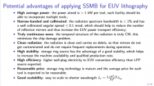
1655736204104.png
1655736068413.png

1655736239294.png

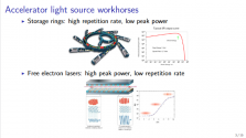
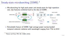
From my point of view looks like they are trying to combine the power characteristic of a Synchrotron with the reliability of a laser.
 

56860

Senior Member
Registered Member
Maybe the Chinese chips industry needs to thank the US for sanctioning China. Another da bai cai in the making.
Please, Log in or Register to view URLs content!
Nineteen of the world’s 20 fastest-growing chip industry firms over the past four quarters, on average, hail from the world’s No. 2 economy, according to data compiled by Bloomberg.
This won't get any attention in the west.

Also there's a Chinese company called 'Great Microwave'.
 

tokenanalyst

Brigadier
Registered Member
Maybe the Chinese chips industry needs to thank the US for sanctioning China. Another da bai cai in the making.
Please, Log in or Register to view URLs content!
American Anti-China Hawks did in a few years what the Chinese government failed to do in almost two decades. That damn irony some advocates of sanctions say "they are necessary they want to stop the Chinese military from accessing advanced semiconductors", call me crazy but following this thread it looks like that they have access to better equipment, software and semiconductors than before that sanctions, because the Chinese military was not buying ASML scanners or Lam research or Applied Materials equipment. CETC was making their own equipment or buying whatever they could find in the Chinese market like SMEE scanners.​
 

ZeEa5KPul

Colonel
Registered Member
View attachment 91219
View attachment 91218

View attachment 91220

From my point of view looks like they are trying to combine the power characteristic of a Synchrotron with the reliability of a laser.
I read these slides before, but I missed that the power was > 1kW per tool. That's amazing. This technology is going to commoditize EUV and China is at the forefront.

2025+ is looking juicy. We should have the first generation Chinese LPP lithography machines by then, which will allow China to access the smallest node sizes. Further along (around 2030), SSMB should become mainstream which will catapult China to the lead in semiconductor manufacturing. Very exciting.
 
Status
Not open for further replies.
Top