Chinese semiconductor industry

Status
Not open for further replies.

tokenanalyst

Brigadier
Registered Member
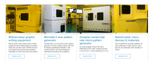
Suzhou Sudavig Technology Group Co., Ltd. (Sudavig for short) is a national high-tech enterprise dedicated to the innovative application of micro-nano key technologies, flexible intelligent manufacturing, and flexible optoelectronic materials.
201705261495777320233.jpg

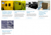
After years of development, Sudavig has become a typical enterprise of independent innovation in the fields of micro-nano optoelectronic materials, new displays and nano-printing, involving micro-nano optical printing materials, nano-printing, 3D imaging materials, flat panel display (large-size capacitive touch screen, ultra-thin conductive Light board), high-end intelligent micro-nano equipment (nano-imprinting, micro-nano direct writing lithography, 3D light field printing, etc.) R & D and industrialization, listed on the Shenzhen Stock Exchange A-share GEM (Su Daweige 300331).
1654274494118.png
1654274522431.png

This guys are less well known, but they do patterning tools for large area micro and nanofabrication but also for IC, MEMs and other areas. They are involved in Maskless direct laser writting lithography and nanoImprint lithography.

Please, Log in or Register to view URLs content!
 

tokenanalyst

Brigadier
Registered Member
development ultra high precision heterodyne interferometry and its use in precision measurement instruments like lithography machines and LIGO type instruments (to measure hecking black holes collision).

Of ultra-precision high-speed laser interferometric displacement measurement technology and instruments.​


In response to the ultra-precision and high-speed displacement measurement requirements put forward in high-end equipment such as microelectronic lithography machines, Harbin Institute of Technology has deeply explored the traditional common optical path heterodyne laser interferometry method and a new generation of non-common optical path heterodyne laser interferometry methods. It has made continuous breakthroughs in many key technologies such as high-precision laser frequency stabilization, precise suppression of optical nonlinear errors, high-speed and high-resolution interference signal processing, and has developed a series of ultra-precision high-speed laser interferometers with the highest relative accuracy of laser vacuum wavelength. 9.6×10 -10 , the displacement resolution is 0.077 nm, the minimum optical nonlinearity error is 13 pm, and the maximum measurement speed is 5.37 m/s. At present, this series of instruments has been successfully used in the field of integrated development and performance testing of lithography machine prototypes with multiple process nodes from 350 nm to 28 nm in my country, providing key technical support and important measurement methods for the development of high-end equipment such as lithography machines in my country.

1654291662947.png

-Testing in litho machines

4.1 Development of domestic lithography machine: multi-axis high-speed ultra-precision laser interferometer​


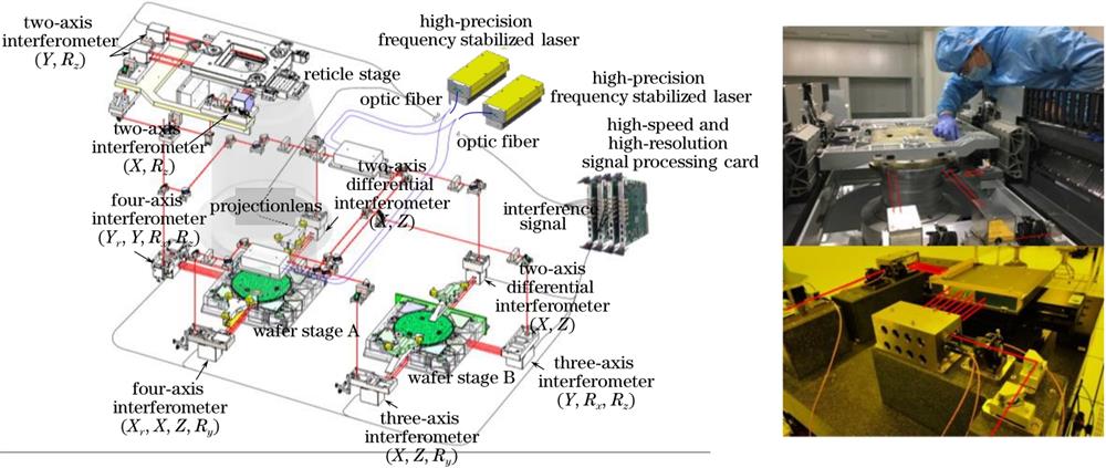
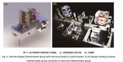
In the development of domestic lithography machines, the multi-axis high-speed ultra-precision laser interferometer is one of the core units embedded in the lithography machine and determines its lithography accuracy. However, on the one hand, European and American countries clearly stipulated that this type of interferometer products are strictly embargoed to my country in the Wassenaar Agreement; Development and production of domestic lithography machines. To this end, our research group has developed a series of ultra-precision high-speed laser interferometry systems, which have been successfully applied in the field of integrated development and performance testing of lithography machine prototypes with multiple process nodes from 350 nm to 28 nm in my country. Typical applications such asFigure 18As shown in the figure, all its key indicators meet the research and development needs of domestic advanced lithography machines, break the embargo blockade imposed by foreign related products on my country, and play an important role in the development of domestic lithography machines. In the applied lithography machine, the number of measurement axes of the interferometer can reach more than 22 axes, the maximum measurement speed can reach 5.37 m/s, and the laser vacuum wavelength/frequency accuracy can reach up to 9.6 × 10 -10 ( k = 3 ), the displacement resolution can reach 0.077 nm, and the minimum optical nonlinearity error is 13 pm. With the ultra-stable constant temperature air bath (3~5 mK@10 min) and vibration isolation environment, the linear displacement and angular displacement can be measured and decoupled synchronously for the multi-dimensional motion of the double workpiece stage in the lithography machine to meet the requirements of the mask. The increasingly complex relative position/attitude measurement requirements between the workpiece table, the silicon wafer workpiece table and the projection objective lens, thereby ensuring the overall overlay accuracy of the lithography machine.​

Schematic diagram of application of ultra-precision high-speed laser interferometry system in lithography machine and field photo

Figure 18. Application principle and on-site photo of ultra-precision high-speed laser interferometry system in lithography machine​

Fig. 18. Schematic diagram of application of ultra-precision high-speed laser interferometry system in lithography machine and field photo​


-Testing in some precision measuring instrument

4.2 Development of National Metrology Benchmark Device: Sub-nanometer Precision Laser Interferometer​


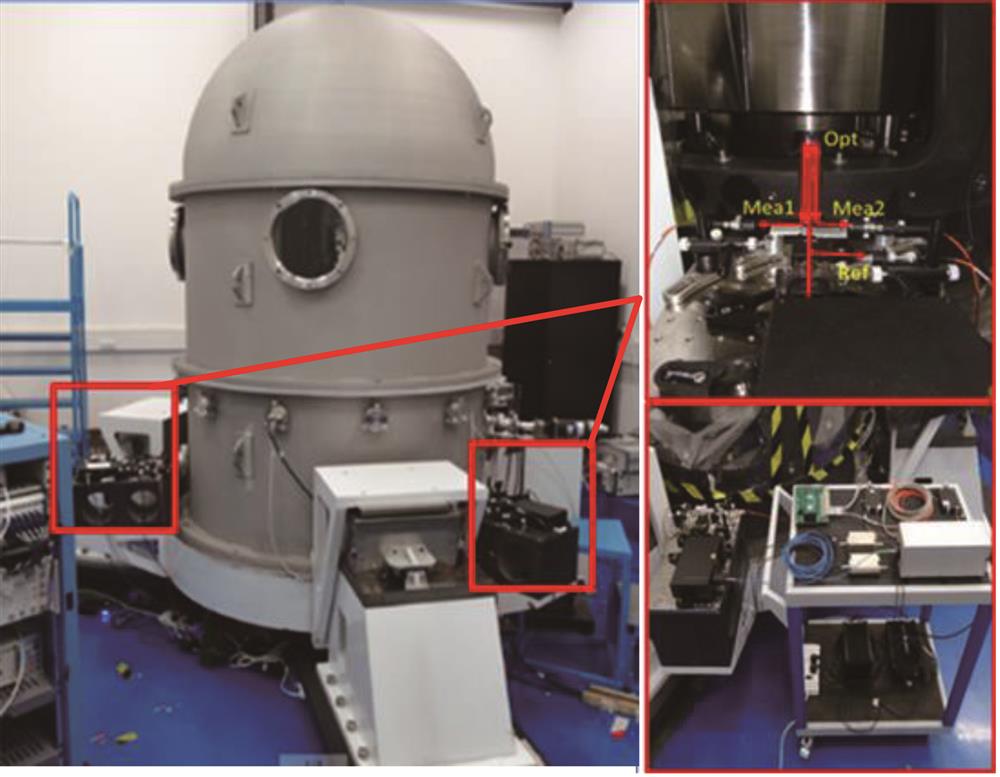
In the development of national-level measurement reference devices, how to use basic physical constants to redefine the mass unit kilogram has been rated as one of the six major scientific problems in the world in recent years by the internationally renowned academic journal "Nature". In the "energy balance" scheme proposed by Academician Zhang Zhonghua of the Chinese Academy of Metrology, one of the key points is to use an ultra-precision laser interferometer to achieve high-accuracy length measurement, which requires an absolute measurement accuracy of less than 1 nm. To this end, our research group developed the first set of sub-nanometer laser interferometers in my country and successfully applied them to the first set of quantized quality benchmark devices in China (Figure 19), played a key role in the implementation of the Chinese scheme of quantized mass benchmarks, and promoted China to become one of the first six countries to successfully participate in the international comparison of kilogram
Please, Log in or Register to view URLs content!
[
Please, Log in or Register to view URLs content!
] . In order to achieve sub-nanometer measurement accuracy, in addition to the precise vibration isolation and temperature control environment, the laser interferometer must be measured in a vacuum environment to exclude the influence of air refractive index on the laser wavelength, and its measurement uncertainty can reach 0.54 nm. @100mm. In addition, in order to realize the attitude monitoring of the measured object, the number of measurement axes of the interferometer reaches 9 axes.

National quantized mass standard and integrated sub-nanometer interferometer

Figure 19. National Quantization Quality Benchmark and its integrated sub-nanometer laser interferometer​

Fig. 19. National quantized mass standard and integrated sub-nanometer interferometer​


Please, Log in or Register to view URLs content!
 

ansy1968

Brigadier
Registered Member
From this YT video, I think this unknown Chinese company Shanghai Sinyang had use the Shanghai Synchrotron Radiation Facility (SSRF) as a tool to research EUV photoresist, it is one of many as Huawei, ICRD, SMIC and others use it and may have some collaboration with CAS (China Academy of Science). The whole of nation approach is starting to bear fruits and the harvesting may take place earlier instead of 2025.

Please, Log in or Register to view URLs content!


Please, Log in or Register to view URLs content!


Please, Log in or Register to view URLs content!

222 views2 hours ago
 

ansy1968

Brigadier
Registered Member
Its been a while, now we return our attention to Huawei as its investment in Chinese tech company are bearing fruits, It had experiencing setbacks BUT its future outlook seems bright. This year is the start of harvest season for Huawei as they prepare for the Return of the King in 2023.

Although facing the chip treaty control of the United States, Huawei has not stopped its action and layout in the chip field. In 2019, Huber Technology Venture Capital Co., Ltd., which focuses on investment in hard technology, was established. So far, Huawei Huber has 78 public investment events and captured many high-quality projects in the semiconductor field. With the maturity of the invested project, Huawei Huber has also ushered in the investment harvest period. Huawei Huber has invested in many chip companies listed this year, such as Novosense, Vanchip and SICC. As of May 6, Huawei Huber has harvested 9 semiconductor projects with IPO, and the cumulative return on investment has reached about 5.2 billion Yuan. On April 22, Novosense, the most expensive chip stock of the year, successfully listed on the Science and Technology Innovation Board of the Shanghai Stock Exchange. Although there was a rare large-scale abandonment of a shares before the IPO, novosense's performance on the first day of listing was quite amazing, with an intraday increase of more than 19%, which not only gave a boost to the continuously depressed A-share market, but also made investors earn huge profits. Novosense's successful IPO has made a number of institutions profitable, including Huawei. Huawei indirectly invested in Novosense in September 2020 through an investment fund called Hongtu Shanli.

Please, Log in or Register to view URLs content!

Please, Log in or Register to view URLs content!

Please, Log in or Register to view URLs content!

Please, Log in or Register to view URLs content!

52 views1 hour ago
 

FairAndUnbiased

Brigadier
Registered Member
From this YT video, I think this unknown Chinese company Shanghai Sinyang had use the Shanghai Synchrotron Radiation Facility (SSRF) as a tool to research EUV photoresist, it is one of many as Huawei, ICRD, SMIC and others use it and may have some collaboration with CAS (China Academy of Science). The whole of nation approach is starting to bear fruits and the harvesting may take place earlier instead of 2025.

Please, Log in or Register to view URLs content!


Please, Log in or Register to view URLs content!


Please, Log in or Register to view URLs content!

222 views2 hours ago
although I like the information about Shanghai Sinyang, this is not a credible source.

The guy doesn't even know how to spell photolithography and spelled it as "photography".

In addition, Shanghai Sinyang is an electrochemistry supplier. For them to do photolithography materials would be a massive leap in capability and change of expertise. Actual photoresist companies typically have done semiconductor precursors in the past.
 

tokenanalyst

Brigadier
Registered Member
Hangzhou Jihai semiconductor's 14nm fab open for bidding. Not domestic equipment though.

Please, Log in or Register to view URLs content!
Winning Bids:

Shenyang Xinyuan Microelectronics Equipment Co., Ltd.
Beijing Xinyidong Technology Co., Ltd.
Nanchang Zhongwei Semiconductor Equipment Co., Ltd.
Shanghai Weisong Industrial Automation Co., Ltd.

Jiangquan Luru Instrument Co., Ltd.

Shanghai Yongying Information Technology Center
(Manufacturer: Huahai Qingke Co., Ltd.)


Lam Research International Sdn.Bhd. (Malaysia)

_Nova Ltd. (Israel)

Rudolph Technologies, Inc. (U.S)

Christie's (China) Co., Ltd.
(Manufacturer: PVA TePla Analytical
Systems GmbH, Germany)

Disco Technology (China) Co., Ltd.
(Manufacturer: DISCO Corporation, Japan)

Agilent Technologies Mouse Easy (Shanghai) Co., Ltd.
(Manufacturer: Agilent Technologies, USA)

KlACorporation

_Pfeiffer vacuum SAS

(Manufacturer: Pfeiffer Vacuum (France) Ltd.,

France)
 

Hendrik_2000

Lieutenant General
Tonyget are you there? Via Vincent progress is being made in localization but it will take sometime to be completely independent from foreign sources. Why is the low rate penetration of ion implanter?
Please, Log in or Register to view URLs content!
How is the progress of localization of semiconductor equipment?

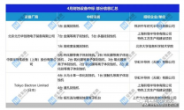
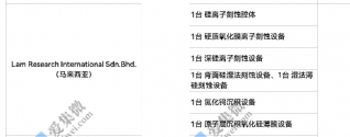
According to the statistics of Weiwang, in April 2022, the number of winning bids for etching equipment in mainland China is 36, of which 26 are domestically produced, namely 14 from North Huachuang and 12 from China Micro.

1654354384901.png

Comment 1:

Obviously, NAURA is strong in the fields of silicon etching and metal etching, while China Micro is leading in dielectric etching, and the respective technical advantages of both parties are quite distinct. In fact, on the whole, there are many types of equipment in the north, and the coverage is wider; the advanced level of Zhongwei is higher. Look forward to the two becoming China's Applied Materials and ASML as soon as possible.

Comment 2:

Not only the etching machine, but the localization data of semiconductor equipment in April is generally quite good: in April, major domestic semiconductor manufacturers purchased 108 equipment, and mainland Chinese manufacturers made a total of 67 equipment, accounting for 62%. Of course, this is closely related to the hot production capacity in the first quarter and the concentrated launch of large-scale production expansion projects.

Comment 3:

From a conservative point of view, April is only a one-month node after all, and the trend depends on the medium and long term, at least 3 months. So what is the situation?

From January to April 2022, major domestic fabs purchased a total of 401 semiconductor equipment, including 97 domestic equipment, and the localization rate is about 24.2% - this is a relatively more realistic total.


From the perspective of long-term data, the current localization rate of etching machines is 20%, cleaning machines 30%, diffusion heat treatment 20%, and CMP 20%, which are all considered high. 90% of the glue remover....The reason everyone knows. The low ones are still 5% for gluing and developing, 5% for thin film deposition equipment, and less than 1% for ion implanters. As for the front lithography machine... not to mention.

Review 4:

It also needs to be viewed from the front. For example, when looking at the data, we should also pay attention to one thing: the proportion of stock or the proportion of incremental.

Because the market stock is too large, even if the speed of localization increases, the incremental proportion is good, and the stock is still very low for a long time. For example, the stock of high-end ion implanters accounted for less than 1%, but in April alone it reached 38.9%. The difference is huge.

The proportion of stock is still low, and the proportion of incremental is gradually rising. And the individual differences are very large: some reach 3nm, most of them reach 14-28nm steadily, and a few have not yet come out of bed.

The former is like this, the latter is slightly better than the former, and the detection is slightly worse than the former.

This is the truer story of the localization of China's semiconductor equipment.
 
Last edited:

caudaceus

Senior Member
Registered Member
A bit out of topic but folks who are working in semiconductor industry, do you have any picture or video that shows what it looks like inside chemical plant that manufacture chemical for semiconductor?
There was a time when I was thinking to enroll in Chemical engineering major. So I still Harbour curiosity to chemical industry in general m
 
Status
Not open for further replies.
Top