Chinese semiconductor industry

Status
Not open for further replies.

tokenanalyst

Brigadier
Registered Member

Research on Correction Technology of Light Field Intensity Distribution of Lithography Machine​

Correction Technology for Illumination Field Intensity Profile in Photolithography Machine
Ma Xiaozhe1,2 Zhang Fang1 ,* Huang Huijie1,2 ,**

1- Laboratory of Information Optics and Optoelectronic Technology Shanghai Institute of Optics and Fine Mechanics Chinese Academy of Sciences Shanghai
2-Center of Materials Science and Optoelectronics Engineering University of Chinese Academy of Sciences Beijing China

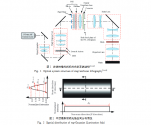
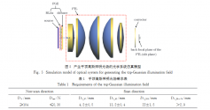
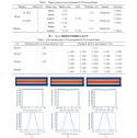
In 28 nm and below node lithography machine, the flat-top Gaussian illumination light field is one of the key technologies to reduce the influence of pulse quantization error on exposure dose. In order to reduce the difficulty in the design, processing and assembly of the flat-top Gaussian illumination light field generating components, a technique for calibrating the illumination light field intensity distribution of a lithography machine is proposed. This technique can obtain a suitable transmittance distribution of the light field correction plate through fewer algorithm iterations, and takes the dimensional tolerance requirement of the intensity distribution in the scanning direction as a boundary condition to reduce the energy loss caused by the correction. The obtained light field correction plate can simultaneously correct the integral uniformity of the illumination light field in the non-scanning direction and the intensity distribution of the light field in the scanning direction. The simulation analysis results show that the light field correction plate obtained by this technology can correct the integral uniformity of the illumination light field in the non-scanning direction to less than 0.29%, and can also correct the intensity distribution in the scanning direction within the index range, and the energy loss introduced by the correction is also reduced. An average reduction of 4.09% can be achieved. The proposed technique can improve the productivity of the lithography machine to a certain extent.​

Please, Log in or Register to view URLs content!

1654208171335.png

1654207777426.png1654207892822.png

Some research and development in the optimization optimization of optics in scan lithography machines.
 

FairAndUnbiased

Brigadier
Registered Member
Just so you know Chinese researchers aren't forgetting the leading edge in terms of process either:

Please, Log in or Register to view URLs content!

Stacked SiGe/Si structures are widely used as the units for gate-all-around nanowire transistors (GAA NWTs) which are a promising candidate beyond fin field effective transistors (FinFETs) technologies in near future. These structures deal with a several challenges brought by the shrinking of device dimensions. The preparation of inner spacers is one of the most critical processes for GAA nano-scale transistors. This study focuses on two key processes: inner spacer film conformal deposition and accurate etching. The results show that low pressure chemical vapor deposition (LPCVD) silicon nitride has a good film filling effect; a precise and controllable silicon nitride inner spacer structure is prepared by using an inductively coupled plasma (ICP) tool and a new gas mixtures of CH2F2/CH4/O2/Ar. Silicon nitride inner spacer etch has a high etch selectivity ratio, exceeding 100:1 to Si and more than 30:1 to SiO2. High anisotropy with an excellent vertical/lateral etch ratio exceeding 80:1 is successfully demonstrated. It also provides a solution to the key process challenges of nano-transistors beyond 5 nm node.

Note that this "beyond 5 nm process" demonstration with GAA architecture was actually done on ancient AMAT 200 mm Producer (first sold in 1998) PECVD, 200 mm Centura CVD (older than Producer), and Lam TCP 9400DFM ICP etcher (first sold in 2000).
 

tokenanalyst

Brigadier
Registered Member
Please, Log in or Register to view URLs content!

Founded in 2001, Jiangsu Lianneng Electronic Technology Co., Ltd. is a professional manufacturer of sensors for vibration testing and dynamic and static testing systems. It is a national high-tech enterprise integrating research, development, production and sales of instruments. It has more than 300 varieties of products in 16 series in four categories.
The company produces various types of sensors, signal conditioners, dynamic and static signal acquisition and analysis systems, modal analysis and vibration and shock excitation and testing instruments, and has a number of invention patents.

Chinese company involved in the R&D and manufacturing of vibration isolation system including active vibration isolation system witch could be necessary to increase performance in some Semiconductor equipment.
 

tokenanalyst

Brigadier
Registered Member
Just so you know Chinese researchers aren't forgetting the leading edge in terms of process either:


Note that this "beyond 5 nm process" demonstration with GAA architecture was actually done on ancient AMAT 200 mm Producer (first sold in 1998) PECVD, 200 mm Centura CVD (older than Producer), and Lam TCP 9400DFM ICP etcher (first sold in 2000).
"WHAT, but I thought that for any structure below 28nm the latest shiniest WFE machine was needed"
 

tokenanalyst

Brigadier
Registered Member

Advanced packaging equipment manufacturer, Taiyan Semiconductor completes a new round of financing​


According to Weibo news, in May this year, Shenzhen Taiyan Semiconductor Equipment Co., Ltd. (referred to as: Taiyan Semiconductor) completed a new round of financing of tens of millions of yuan. Investors include Meihua Venture Capital and Hechuang Capital.

It is reported that Taiyan Semiconductor is a semiconductor process and equipment service provider based in the field of advanced packaging. The core team has many years of experience in equipment manufacturing and process in the semiconductor industry. In August 2019, Shenzhen Taiyan Semiconductor Equipment Co., Ltd. was reorganized and established. Its official news shows that Taiyan provides Laser + Plasma + Sputter composite technology as its core technology, focuses on process application equipment related to advanced packaging processes such as SiP, Fanout, 3D WLP, and provides Sputter target application services, which can be used for advanced packaging in the market. The industry provides complete equipment solutions.

According to Xueyu Capital news, Zhang Shaobo, general manager of Taiyan Semiconductor, said that after this round of financing, the funds will be mainly used to expand and set up production lines. For the company's products, we can provide customers with a complete production line with a complete set of back-end processes.

At present, Taiyan Semiconductor has three types of packaging equipment: sputtering equipment, laser equipment, and plasma equipment.

At the same time, Taiyan Semiconductor is also actively deploying related intellectual property rights such as semiconductor equipment, processes, materials, and automation. At present, the company has ISO9000 quality management system certification, and a number of patents are mainly used in system-in-package (SiP), fan-out packaging (Fanout), vacuum Sputtering (Sputter), plasma technology (Plasma), laser technology (Laser) and other fields. (Proofreading / Xiaobei)

Please, Log in or Register to view URLs content!
 

tokenanalyst

Brigadier
Registered Member

Taiwan bans all modern chip exports to Russia, Belarus​


It is reported that China's Taiwan region has banned the sale of modern chips to Russia and Belarus in response to Ukraine's invasion.

This week, Taiwan's Ministry of Economic Affairs (MOEA) released a list of strategic high-tech products banned from exporting to Russia and Belarus, DigiTimes reported. The ministry said the high-tech goods were also banned from Belarus because it could help Russia bypass sanctions.

Companies in both countries are now prohibited from purchasing Taiwan-made microprocessors or microcircuits with any of the following specifications:

The chip reaches a speed level of more than 5gigaflops, or the capacity of the arithmetic logic unit is more than 32bit;

The clock frequency of electronic components exceeds 25 MHz;

• One or more ports or interfaces provide transfer rates greater than 2.5 MB/s between components.

• High-speed microcircuits with more than 144 contacts.


- basically anything , why even bother to make a list?

These conditions essentially exclude Russia and Belarus from modern technology made in Taiwan. In addition, Taiwan, China will no longer sell chip production equipment to these countries. This includes alignment and exposure equipment, scanners and scanning electron microscopes for wafer production.

-What important SME equipment manufacturers Taiwan have? I think they buy most of their equipment from other countries.

Well now Russia will be more willing to sell what China wants.
 

FairAndUnbiased

Brigadier
Registered Member

Taiwan bans all modern chip exports to Russia, Belarus​


It is reported that China's Taiwan region has banned the sale of modern chips to Russia and Belarus in response to Ukraine's invasion.

This week, Taiwan's Ministry of Economic Affairs (MOEA) released a list of strategic high-tech products banned from exporting to Russia and Belarus, DigiTimes reported. The ministry said the high-tech goods were also banned from Belarus because it could help Russia bypass sanctions.

Companies in both countries are now prohibited from purchasing Taiwan-made microprocessors or microcircuits with any of the following specifications:

The chip reaches a speed level of more than 5gigaflops, or the capacity of the arithmetic logic unit is more than 32bit;

The clock frequency of electronic components exceeds 25 MHz;

• One or more ports or interfaces provide transfer rates greater than 2.5 MB/s between components.

• High-speed microcircuits with more than 144 contacts.


- basically anything , why even bother to make a list?

These conditions essentially exclude Russia and Belarus from modern technology made in Taiwan. In addition, Taiwan, China will no longer sell chip production equipment to these countries. This includes alignment and exposure equipment, scanners and scanning electron microscopes for wafer production.

-What important SME equipment manufacturers Taiwan have? I think they buy most of their equipment from other countries.

Well now Russia will be more willing to sell the China wants.
Ironically their stated restrictions means Russia can buy aerospace grade chips such as IBM RAD6000 lmao.

Please, Log in or Register to view URLs content!
 

gelgoog

Lieutenant General
Registered Member
Russia can make better chips than that by itself. Mikron produces the Elbrus-2SM at 300 MHz.
If they really wanted to, they could likely manufacture 2 GHz processors or better with their existing equipment.

Also, Russia just announced their first counter sanctions with regards to the semiconductor sector.
Note: the three major world suppliers of neon are Ukraine, Russia, and China.

Please, Log in or Register to view URLs content!

Inert gas export restriction to strengthen Russia’s position on microelectronics market​

Russia restricted exports of inert gases, including neon, to unfriendly states in late May

MOSCOW, June 2. /TASS/. The restriction of inert gases export will strengthen Russian positions on the global microelectronics market, Deputy Minister of Industry Vasily Shpak told TASS.
Russia restricted exports of inert gases, including neon, to unfriendly states in late May. Such gases comprise in particular argon and helium used in production of semiconductors.

Please, Log in or Register to view URLs content!
... roughly 70% of 540,000 metric tons of neon produced in the world is used in semiconductor chip manufacturing. This high demand exists because neon is an essential, irreplaceable, and major component of argon-fluorine-neon excimer pulsed lasers. Note that excimer is the abbreviation for excited dimer — see below.

This class of lasers are renowned for their high-intensity, pulsed, nanosecond, 193 nm-deep ultraviolet wavelength output, as well as their very small diffraction-limited spot size, pivotal for state-of-the-art 7 nm spatial resolution photolithography. They are used mainly in computer chip production but have a myriad of other uses, including laser weaponry, nuclear fusion, sub-micron machining, isotope separation, and eye surgery.

Notably, two Ukrainian companies, Ingas and Cryoin, are responsible for the production of around 50% of the global supply of semiconductor grade neon for chip-making excimer lasers. Puzzling is why this kind of excimer laser is so hungry for neon, as one imagines the active argon-fluorine-neon gaseous blend contained in the laser cavity would not be consumed.

Please, Log in or Register to view URLs content!

Before the invasion, Ingas produced 15,000 to 20,000 cubic meters of neon per month for customers in Taiwan, Korea, China, the United States and Germany, with about 75% going to the chip industry, Nikolay Avdzhy, the company's chief commercial officer, said in an email to Reuters.

The company is based in Mariupol, which has been under siege by Russian forces. On Wednesday, Russian forces destroyed a maternity hospital there, in what Kyiv and Western allies called a war crime. Moscow said the hospital was no longer functioning and had been occupied by Ukrainian fighters.

Please, Log in or Register to view URLs content!

Chip companies and industry analysts say there’s anywhere between one to six months worth of neon in reserve. If that runs out, these companies won’t be able to make semiconductors.
 
Last edited:

ansy1968

Brigadier
Registered Member
Russia can make better chips than that by itself. Mikron produces the Elbrus-2SM at 300 MHz.
If they really wanted to, they could likely manufacture 2 GHz processors or better with their existing equipment.

Also, Russia just announced their first counter sanctions with regards to the semiconductor sector.

Please, Log in or Register to view URLs content!

Inert gas export restriction to strengthen Russia’s position on microelectronics market​

Russia restricted exports of inert gases, including neon, to unfriendly states in late May

MOSCOW, June 2. /TASS/. The restriction of inert gases export will strengthen Russian positions on the global microelectronics market, Deputy Minister of Industry Vasily Shpak told TASS.
Russia restricted exports of inert gases, including neon, to unfriendly states in late May. Such gases comprise in particular argon and helium used in production of semiconductors.
"We have sufficient capabilities, we are present on this market. We also plan to increase production capacities in the near future. We believe we will have an opportunity of being heard in this global chain and this will provide us with certain competitive advantages, if there is a need for mutually beneficial talks with colleagues," the official said.
Inert gases are among base materials for production of semiconductors, Shpak said.

"About 4,000 various materials and chemicals are used to produce semiconductors, speaking about the process. However, there are basic things present with actually all the producers in the process - in particular, these are high-purity gases, especially neon," he noted.
The crisis with semiconductors started long before the pandemic and the decision on inert gases export restrictions "will enable chains turned out to be disrupted for the time being in a new fashion," the official added.
@gelgoog bro you beat me to the punch, I think the Virgin Heroine doesn't expected this...lol, who suffered the most, Russia can replace that with Chinese import cause they don't need 7nm and 5nm chips, can Taiwan semiconductor industries survived w/o the Russia who supply 30% of the world demand. @supersnoop is correct, this kind of identity politics will ruin the Collective West from within, the virtuous signaling create an opposite effect cause the outcome is suffering. All in all the winner is China and the Chinese didn't need to act as the Collective West give away such opportunity in a silver platter...lol and perfect timing as the Chinese IC is expanding in an accelerating rate.
 
Status
Not open for further replies.
Top