Chinese semiconductor industry

Status
Not open for further replies.

tonyget

Senior Member
Registered Member
Second hand equipment? Those new SMIC 28nm fabs are just begin to construct,let alone move in equipments. Just check all recent bidding information from SMIC,all of which are for designated for existing SMIC fabs.

Production bottleneck has nothing to do with equipment for specific node,does it take longer to make 14nm equipment compare to 28nm equipment?Does production bottleneck only applys to 14nm products but not 28nm products?

Yes. You can use second hand or older equipment that is already in stock for 28 nm equipment. 14 nm equipment is newer by definition, there are less second hand ones on the market and new ones are being sold.

For etch and deposition, X nm equipment isn't exclusively for that process node since they don't go by etch/deposition chemistry. FinFET requires different types of etch and deposition chemistry than planar. Etch and deposition tools suitable for FinFET are competing with other major customers, while those suitable for planar processes aren't.

Please, Log in or Register to view URLs content!

Production bottleneck is being seen all over the world, this is not an unbacked claim. Lead times went from 6 months to 8 months in 2021 and 18 months in 2022.

Please, Log in or Register to view URLs content!

Please, Log in or Register to view URLs content!

I suggest you familiarize yourself with industry literature and trends before making sweeping conclusions. We have given you a wealth of information that makes it easy to understand the industry.
 

Annihilation98

Junior Member
Registered Member
SMIC I believe they can't move to higher nodes because more than 90% of their equipment is manufactured by US companies. They already got sanction and are still stuck with 14nm despite almost 3 years of research to move to higher nodes. Their 14nm is still not at the same level as TSMC or Samsung 14nm tech. In the semiconductor industry, the most notable semi equipment companies like KLA Tencor, Lam Research, Applied Materials, and ASML are already prepared to not supply China with any advanced technology.

ASML EUV machine:

Carl Zeiss EUV lenses Worlds's flattest lenses
 
Last edited:

FairAndUnbiased

Brigadier
Registered Member
Second hand equipment? Those new SMIC 28nm fabs are just begin to construct,let alone move in equipments. Just check all recent bidding information from SMIC,all of which are for designated for existing SMIC fabs.

Production bottleneck has nothing to do with equipment for specific node,does it take longer to make 14nm equipment compare to 28nm equipment?Does production bottleneck only applys to 14nm products but not 28nm products?
How about provide us with the bidding list so everyone can see what data you reference?

The existence of second hand 28 nm suitable equipment means that new ones have lower demand. Lower process requirements means more equipment is suitable. This is very simple logic.

Deciding what node to build depends primarily on customer demand at SMIC. Itis very academic for you to say only highest node should be built but what's the business case? Of 28 nm + FinFET how much is 28 nm, how much is FinFET? You don't know, I don't either.

The demand at SMIC doesn't necessarily match the demand of the market as a whole. How come nobody says Texas Instruments is a stone age company because they don't even have a single FinFET fab? Exactly.

Please, Log in or Register to view URLs content!

How come Texas Instruments is focusing on 45 nm fab? They have 28 nm products but focus on 45 nm fab. I guess by your logic it must be because their 28 nm process is shit and useless, not because they have a better business case for 45 nm and more demand at 45 nm.
 

tokenanalyst

Brigadier
Registered Member
the most notable semi equipment companies like KLA Tencor, Lam Research, Applied Materials, and ASML are already prepared to not supply China with any advanced technology.
No they are not prepare, nothing prepare a company to lose a 1/4 of their profits, losing decades of reputation of being a reliable supplier and what is worse: the encouragement of local competition in a niche market like SME were clients are just a few.
So prepare they are that they are willing to move production overseas to avoid excessive export controls because American companies like LAM, KLA, AM know that they are going to be the biggest losers. different from ASML EUV what they made is not irreplaceable.

Please, Log in or Register to view URLs content!
 

tokenanalyst

Brigadier
Registered Member
How about provide us with the bidding list so everyone can see what data you reference?

The existence of second hand 28 nm suitable equipment means that new ones have lower demand. Lower process requirements means more equipment is suitable. This is very simple logic.

Deciding what node to build depends primarily on customer demand at SMIC. Itis very academic for you to say only highest node should be built but what's the business case? Of 28 nm + FinFET how much is 28 nm, how much is FinFET? You don't know, I don't either.

The demand at SMIC doesn't necessarily match the demand of the market as a whole. How come nobody says Texas Instruments is a stone age company because they don't even have a single FinFET fab? Exactly.

Please, Log in or Register to view URLs content!

How come Texas Instruments is focusing on 45 nm fab? They have 28 nm products but focus on 45 nm fab. I guess by your logic it must be because their 28 nm process is shit and useless, not because they have a better business case for 45 nm and more demand at 45 nm.
1653916153152.png
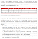
According to this translation the localization for bids in SMIC lastest fab is about 45% (is really high) but that doesn't mean that the rest of the suppliers are American, TEL has been winning orders, also Koreans, Singaporean and other Asian equipment manufacturers.
 
Last edited:

tokenanalyst

Brigadier
Registered Member

Zhaochi Semiconductor's new Unimax equipment has been debugged and the epitaxial wafer has been successfully lit, and the expansion of Mini LED production has accelerated​


According to the news from Weinet, Jiangxi Zhaochi Semiconductor Co., Ltd. , on May 27, the company's new Unimax equipment was debugged and the epitaxial wafer was successfully lit up, marking the smooth progress of Zhaochi Semiconductor's production expansion plan and the expansion of Mini LED production. Speed up.

16538920104690.png


It is reported that since the signing of the contract, the expansion plan of Zhaochi Semiconductor has been progressing smoothly. The first batch of equipment entered the factory for debugging last month and was officially lit on May 27. After this verification, the follow-up equipment will be delivered to the factory in batches, and the supporting flat film, PSS and chip equipment will also be expanded as planned.

Official news shows that the previously announced production capacity of 1 million pieces is expected to be reached in the first quarter of 2023.

The Unimax epitaxy equipment purchased in this round of production expansion is the leading epitaxy MOCVD equipment in China, and it has excellent wavelength uniformity. With more stable mass production performance.
 

gelgoog

Brigadier
Registered Member
Production bottleneck has nothing to do with equipment for specific node,does it take longer to make 14nm equipment compare to 28nm equipment?Does production bottleneck only applys to 14nm products but not 28nm products?
The amount of tools you need to make 28nm wafers is different from the amount you need to make lower resolution wafers. See @tinrobert 's article at Seeking Alpha. You need like twice the amount of lithography machines for the FinFET processes at 7nm. And ASML currently has a well known problem with delivering lithography machines to meet existing orders. Not just EUV machines but also DUV ones. Which are the ones SMIC uses.

SMIC I believe they can't move to higher nodes because more than 90% of their equipment is manufactured by US companies. They already got sanction and are still stuck with 14nm despite almost 3 years of research to move to higher nodes. Their 14nm is still not at the same level as TSMC or Samsung 14nm tech. In the semiconductor industry, the most notable semi equipment companies like KLA Tencor, Lam Research, Applied Materials, and ASML are already prepared to not supply China with any advanced technology.
China already has its own replacements for most of the equipment companies like Lam Research, Applied Materials, or Tokyo Electron make. Those Chinese equipment companies have plans to like double existing production of tools in the short term and are growing at 33% annual growth rates or higher.

We have fairly reliable information that SMIC has achieved 90% or better yields on 14nm FinFET process. That means they are economically competitive with TSMC in that process. The process is in mass production. We also had information, before the US sanctions hit big time, that customers taped out N+1 designs at SMIC. Now, that does not happen unless you are going to do tentative production of N+1. So you can be fairly certain that N+1 is also at least in the risk production status if not better than that. First N+1 wafers should have been delivered to customers a long time ago.
Please, Log in or Register to view URLs content!

@tinrobert estimates in his article that N+2 should also be in production right now at SMIC given historical development trends at other companies.
 
Last edited:

tokenanalyst

Brigadier
Registered Member

Integrated device of electrostatic chuck and manufacturing method​

CN114496891A
2022

Abstract​

The invention relates to the technical field of electrostatic chucks, in particular to an integrated device of an electrostatic chuck and a manufacturing method thereof. The integrated device of the electrostatic chuck comprises a vacuum cavity and a vacuum pumping system, wherein the vacuum cavity comprises an upper cavity and a lower cavity which are separated by a partition plate; the vacuum pumping system is connected with the upper chamber and the lower chamber; the vacuum pumping system comprises a first vacuum pump pipeline, a second vacuum pump pipeline, an air charging pipeline, an exhaust pipeline and a vacuum pipeline. The electrostatic chuck manufactured by adopting the device and the method has the characteristics of high bonding strength, no air bubbles and the like, and all bonding layers are uniform; the edge and the internal heat conductivity coefficient are consistent, the temperature uniformity of the electrostatic chuck cannot be influenced, and the defect control of large-area bonding is better.

The invention relates to the technical field of electrostatic chucks, in particular to an integrated device of an electrostatic chuck and a manufacturing method thereof.

Background
The electrostatic chuck is a stage of a wafer precision machining apparatus, and is often arranged in a PVD coating apparatus, an etching apparatus, an ion implantation apparatus, an EUV lithography apparatus, and the like, and is one of core components of the above apparatuses.

1653928121801.png

Please, Log in or Register to view URLs content!

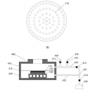
U-precision patent in electrostatic chucks ( a wafer holding device using electrostatic force) for equipment that need to use vacuum for operation like EUVL.
 

ansy1968

Brigadier
Registered Member

Integrated device of electrostatic chuck and manufacturing method​

CN114496891A
2022

Abstract​

The invention relates to the technical field of electrostatic chucks, in particular to an integrated device of an electrostatic chuck and a manufacturing method thereof. The integrated device of the electrostatic chuck comprises a vacuum cavity and a vacuum pumping system, wherein the vacuum cavity comprises an upper cavity and a lower cavity which are separated by a partition plate; the vacuum pumping system is connected with the upper chamber and the lower chamber; the vacuum pumping system comprises a first vacuum pump pipeline, a second vacuum pump pipeline, an air charging pipeline, an exhaust pipeline and a vacuum pipeline. The electrostatic chuck manufactured by adopting the device and the method has the characteristics of high bonding strength, no air bubbles and the like, and all bonding layers are uniform; the edge and the internal heat conductivity coefficient are consistent, the temperature uniformity of the electrostatic chuck cannot be influenced, and the defect control of large-area bonding is better.

The invention relates to the technical field of electrostatic chucks, in particular to an integrated device of an electrostatic chuck and a manufacturing method thereof.

Background
The electrostatic chuck is a stage of a wafer precision machining apparatus, and is often arranged in a PVD coating apparatus, an etching apparatus, an ion implantation apparatus, an EUV lithography apparatus, and the like, and is one of core components of the above apparatuses.

View attachment 89723

Please, Log in or Register to view URLs content!

U-precision patent in electrostatic chucks ( a wafer holding device using electrostatic force) for equipment that need to use vacuum for operation like EUVL.
@tokenanalyst bro great find, official confirmation of the DUAL BENCH develop by U- Precision, one of the 3 core component for EUVL, the other is optics by CIOMP both had been successfully develop. while waiting for the 3rd which is the light source, China is working on 4 possible solution as urgency dictate the need for an operational EUVL.

1)CIOPM (Changchun Institute of Optics and Mechanics) Dual wavelength laser coaxial output system.

2) CAS (China Academy of Science) Institute of High Energy Physics develop an adjustable Extreme Ultraviolet light source tech? Adjustable?

3)Sichuan University develop a 13.5 light source that can be use on DUVL, EUVL and other high end Lithography body, a LPP?

4)finally the SSMB
 

Annihilation98

Junior Member
Registered Member
China already has its own replacements for most of the equipment companies like Lam Research, Applied Materials, or Tokyo Electron make. Those Chinese equipment companies have plans to like double existing production of tools in the short term and are growing at 33% annual growth rates or higher.
We all know China has replacement equipment but its not same level as US. Probably not enough to make even sub 20nm nodes. To make sub 10nm nodes, its not just about EUV, its the combination of other state of art equipment of respective company.
 
Status
Not open for further replies.
Top