After France its Brazil turn to go Huawei 
113 views1 hour ago
113 views1 hour ago
It's risky. Like they said, since Huawei is doing the final packaging there's 2 different types of failures that can occur: design failures and process failures. Huawei will definitely need to embed a ton of test and debug features for both individual chips and the assembled package if they want to go this route.@tokenanalyst ,@Oldschool ,@WTAN @foofy and @FairAndUnbiased , brothers I have a crazy question so do bare with me, IF its possible that Huawei or Hisilicon let SMIC fab an unfinished 14nm chips and they're the one to finished the packaging as they had done with TSMC 5nm chips that led to kirin 9006C. In this way they may circumvent the sanction by stating the Chip as unfinished product thus not recorded?
5nm Kirin 9006C chip comes out, Huawei successfully breaks through again
2022-05-04 18:58 HKT
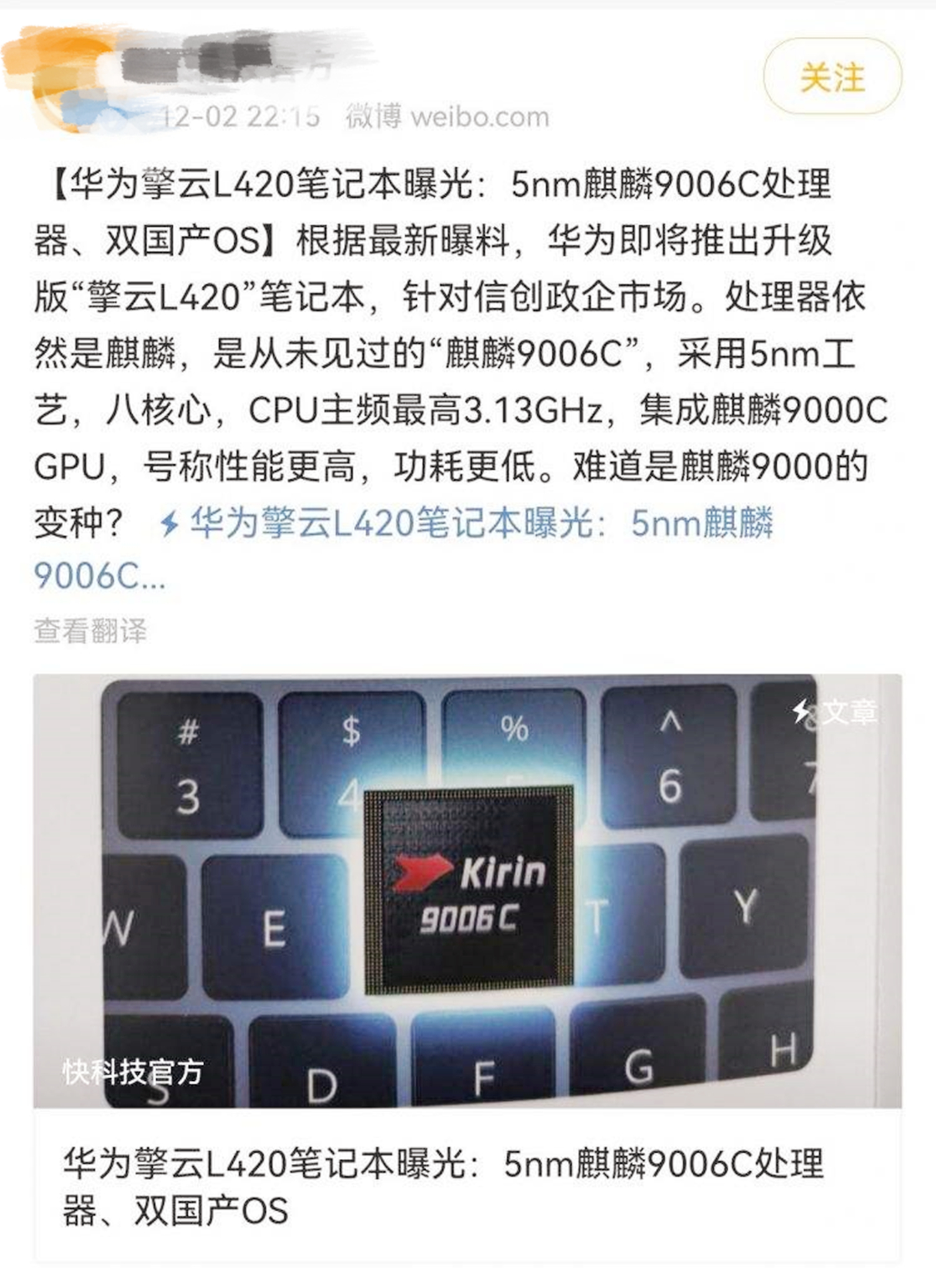
Many people speculate that Huawei may have broken through the chip blockade of Eagle Sauce , because recently Huawei's new products use a Kirin chip that has never been seen before. This chip is called Kirin 9006 .
What makes many people wonder is how this chip was made? We must know that the current blockade of Huawei by Yingjiang has not relaxed at all. Who is so bold and antagonistic to Yingjiang?
Huawei's precautions
In fact, everyone has misunderstood that although this chip has just come out, but these chips are not just out of the library, but from Huawei's inventory. This Kirin 9006 chip still uses TSMC technology, and this chip is still the top 5nm process . In terms of structure and performance, Kirin 9006 series chips and Huawei's Kirin 9000 belong to the same brothers , and the similarity between the two is very high in these aspects.

In fact, after Eagle Sauce gave Huawei an ultimatum, Huawei, which was unwilling to give in, could only ask TSMC to produce as many chips as possible for itself at the last moment , so that it could hold on for a while when Eagle Sauce suppressed in the future. time. However, at this time, Huawei encountered a serious problem. At that time, Huawei was developing the Kirin 9006 chip, but this chip had not been thoroughly designed yet, and many structures of the chip needed to be perfected, and it had not yet reached the standard for mass production.
But at this time, Huawei knows that if the chip cannot be mass-produced in a short period of time, then this chip will probably stay on the drawing forever, and there will never be a way to be manufactured . This situation is completely unacceptable for Huawei. Huawei has spent a lot of money to develop this chip. If this chip fails at this time , it means that all of Huawei's early investment will be in vain and become meaningless . This will make Huawei, which is already struggling to make a profit this year, even more cramped in the capital chain. So at this time Huawei made a major decision.
Risky decision
Huawei's risky decision is to let TSMC directly produce the Kirin 9006 chip according to Huawei's current progress in the design of the Kirin 9006 chip . This decision surprised many people. Because this means that even if the Kirin 9006 chip is mass-produced, the obtained chip cannot be used in the product immediately , because it is basically a semi-finished product, and the design of many parts is not complete.
Huawei's idea is that since the overall framework of the chip has been laid out, it is better to build the chip first , so that the chip will not be completely stuck on the drawing and there is no way to mass produce it. As for the flaws and deficiencies in the chip design process, Huawei can make up and improve in the future, so that this chip will finally have the strength to carry .
In fact, this is a very risky decision.
First of all, Huawei does not know whether there are loopholes in the design of this chip . Because this chip has not been officially taped out and has not undergone performance testing, Huawei does not know whether there are design flaws in the design of this chip. At this time, it is a very risky decision for Huawei to mass-produce this chip . Because once discovered in the later stage, this chip has design flaws , it is very likely that this chip can not be put into practical applications in the end, which will be a huge loss for Huawei .
Secondly, whether Huawei has the technical strength to perfect these semi-finished chips and finally apply them to the use of products , these are questions that have to be considered. However, in the end, in order to be able to win more capital for the turnaround , Huawei resolutely put this chip into mass production.
Huawei ushered in new opportunities
Facts have proved that Huawei's decision is correct. After several months of hard work, Huawei has relied on its strong technical strength to perfect all of these Kirin 9006 chips . At present, these chips can already be used in products. Through performance testing, Kirin 9006 is superior to Huawei's previous flagship Kirin 9000 in all aspects . It can be seen that Kirin 9006 may help Huawei achieve a new round of technological breakthroughs in the future.
At present, Huawei's latest laptop "Qingyun L420" has begun to carry the low-profile version of the Kirin 9006C of this chip. According to user feedback, this laptop is equipped with Huawei's latest chip, which is superior in performance, fluency, and power consumption. The performance is very good . The advent of the Kirin 9006 caught Eagle-chan by surprise. No one thought that a few months later, Huawei could actually pull out a hole card at this time . It seems that Eagle-chan's desire to defeat Huawei in one fell swoop was completely shattered .
Huawei's foresight has given itself more capital to turn around when fighting against Yingjiang's suppression. Of course, these can only help Huawei persist for a longer time. In the future, if Huawei wants to go more smoothly, it still has to achieve technological breakthroughs. Therefore, we must expect Huawei to make more efforts.
5nm Kirin 9006C chip came out, Huawei once again demonstrated its own strength
Unexpectedly, Huawei still has a hole card! 5nm chip came out, Huawei successfully turned over
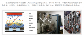
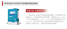
And there we have it.An EUV radiation source generating device for lithography machine
Patent Type:
Invention Disclosure
Application (patent) number:
CN202210069647.4
Application Date:
2022-01-21
Application publication number:
CN114397799A
Public announcement date:
2022-04-26
Sovereign item:
1. an EUV radiation source generating device for a lithography machine, comprising a conveyor belt; it is characterized in that: also comprising an EUV radiation source generating unit, a cleaning unit, a fuel injection unit, a vacuum control unit; the EUV radiation source generating unit includes A reflective cup sleeved on the conveyor belt and a laser set under the reflective cup; the lower part of the reflective cup is provided with an arc-shaped seal, and a laser emission hole matched with the laser is provided on the seal; on the belt body of the conveyor belt A light-passing hole is arranged, a laser crystal is arranged in the light-passing hole, a coating layer is arranged on the upper part of the laser crystal, a plurality of micrometer holes are arranged on the coating layer, and a fuel capable of generating extreme ultraviolet light is arranged in the micrometer hole; The laser is provided with a probe that can identify colors; the cleaning unit includes a debris cleaning cavity sleeved on the conveyor belt, and the conveyor belt inside the debris cleaning cavity is provided with a loop; a steam spray head is arranged in the cleaning cavity, and the steam spray head Corresponding to the laser crystal on the top of the ring; the fuel injection unit includes a fuel injection cavity, and a high-pressure nozzle is arranged in the fuel injection cavity, and the high-pressure nozzle is communicated with the fuel liquid storage tank and corresponds to the micron hole; The front part of the injection cavity is provided with a first mechanical arm and an auxiliary light source, the first mechanical arm is used for moving the photosensitive block on the laser crystal, and the auxiliary light source is used for emitting a light beam to the laser crystal to break down the photosensitive block ; A second mechanical arm is arranged at the rear of the fuel injection cavity, and the second mechanical arm is used to remove the photosensitive block.
Summary:
The invention discloses an EUV radiation source generating device for a lithography machine, comprising a conveyor belt; it is characterized in that: it further comprises an EUV radiation source generating unit, a cleaning unit, a fuel injection unit, and a vacuum control unit; the EUV radiation source generates The unit includes a reflector and a laser; a light-passing hole is arranged on the belt body of the conveyor belt, a laser crystal is arranged in the light-passing hole, a coating layer is arranged on the upper part of the laser crystal, and a plurality of micron holes are arranged on the coating layer. A fuel capable of generating extreme ultraviolet light is arranged in the micron hole; the cleaning unit includes a debris cleaning chamber and a steam nozzle; the fuel injection unit includes a fuel injection chamber and a high-pressure nozzle; a first mechanical arm is arranged in front of the fuel injection chamber and an auxiliary light source, and a second mechanical arm is arranged at the rear of the fuel injection cavity. The invention effectively realizes the continuous operation of the device, ensures the reliability of fuel filling, improves the production efficiency of the device, and simultaneously achieves the purpose of improving the lithography precision.
Everyone in the industry knows the jargon. Doesn't make them 100% accurate, also doesn't make them an expert at all sectors in the semiconductor industry. I've always been clear about my limits of understanding. It helps to be clear about this, to ensure that people understand what is conjecture and what isn't.Which is exactly my point, why bother refitting ASML machines? It's a waste of time and money that should be going into optimizing and developing SMEE lithography machines. China has indigenous 28nm/14nm capability with the SSA800 (what it doesn't have yet is volume); work should continue on that so China can move into 7nm/5nm with a refined DUVL successor within a year or so.
Personally, I have a higher bar to clear than some technical jargon. Plenty of trolls - and plenty of the alts of one particularly persistent troll - have used technical jargon to obfuscate unsound and bad faith arguments. Even if I grant that this person has domain expertise, that doesn't entail that he has the first clue what the Chinese lithography industry is capable of or what it's doing. To understand that we need first hand sources and those have dried up, unfortunately.
Furthermore, there are other users in this thread with at least the same grasp on the jargon who disagree with him, so his positions are controversial even on interpretations far more charitable than I'm inclined to give.
Please argue with some sense here, don't degrade this thread.Good to know that you recognise Taiwan as a country
Sorry guys, got the dates wrong. Thought this was present.Please argue with some sense here, don't degrade this thread.

These are very high end custom instruments for semiconductor RD to pilot scale production/metrology.Shenyang Keyou Vacuum Technology Co., Ltd. specializes in the research, development and manufacture of vacuum equipment and instruments. The legal representative is General Manager Qu Hongbo. The company was established in 2006, formerly known as Shenyang Keyou Vacuum Technology Research Institute. comprehensive enterprise.
The new site of the company is located in Sujiatun District, Shenyang City, close to Shenying Highway, and can be directly connected to Taoxian Airport, Shenhuan Expressway, etc. nearby, with superior geographical location and convenient transportation. Our company has more than 50 employees, with a total of 6,200 square meters of modern industrial plants, offices and other auxiliary facilities, and more than 50 sets of various advanced processing equipment and testing instruments.
The company's products and business scope mainly include:
vacuum equipment design solutions; high vacuum, ultra-high vacuum thin film preparation equipment; vacuum smelting and heat treatment equipment; time-of-flight mass spectrometer, optoelectronic imaging equipment, laser mass spectrometer and other analytical instruments; nanomaterial preparation equipment ;Industrial product manufacturing equipment; Ion beam etching equipment; Vacuum valves, vacuum components; Electronic control, high pressure, temperature control, power supply and other components In addition, to undertake other vacuum equipment or instruments, design, products, technical services.
View attachment 88254
