I try to not claim personal authority and only discuss the science here. I don't like claims of personal experience because it can't be verified and may violate NDAs both explicit and implicit. In the end I don't think of my job as ideological, it's a mildly interesting thing I get paid for, so I don't take risks.It might be, @hvpc and @FairAndUnbiased they know their stuff, but I have trouble believing that fabs workers go around telling people outside the things that happen in their work environment and much less very sensitive information like new equipment. That will mean a lack of discipline in the industry and possible breach of contracts.
You are using an out of date browser. It may not display this or other websites correctly.
You should upgrade or use an alternative browser.
You should upgrade or use an alternative browser.
Chinese semiconductor industry
- Thread starter Hendrik_2000
- Start date
- Status
- Not open for further replies.
BG-607 automatic double-sided lithography machine introduction (CETC)
the BG-607 six-inch automatic double-sided lithography machine is grandly launched. This model has automatic loading and unloading, automatic double-sided alignment, automatic precision leveling, and high uniformity. Ultraviolet light source, gap exposure and other characteristics, various technical indicators have reached the domestic leading level, and can be applied to power devices, optoelectronic devices , filter devices, thin film devices and MEMS and other fields.
The fully automatic double-sided alignment system adopts industrial-grade cameras, high-definition and high-magnification optical lenses, and advanced visual algorithms, which are suitable for automatic identification and alignment of various marks; the self-developed bottom alignment system can reliably ensure the precision of bottom graphics carve.
The fully automatic transmission system adopts the double-arm manipulator, which realizes the star-shaped three-dimensional transmission of the cassette, pre-alignment, and alignment worktable.
The wafer pre-alignment system adopts a multi-function calibrator, which can efficiently and quickly complete the center positioning and trimming alignment of the wafer; three-axis centering, correcting the wafer positioning edge and center; sensor recognition, reducing the contact to the wafer.
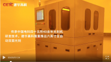
Looks like and upgrade from this automated mask aligner
To think the mask aligners are still a thing in the era of scanners, steppers and now maskless lithography. Is like the radio, its never dies.
Not the greatest site to link for obvious reason but I can’t find any other decent articles.
It’s not directly related to China semi industry but more indirectly related.
The Japanese and U.S. governments are close to agreeing to cooperate in the production of chips using 2-nm (nanometer) technology and even more advanced solutions. Both countries are concerned about their dependence on Taiwanese and other suppliers and are seeking to diversify their sources. They are also working on a mechanism to prevent technology leakage, especially in China.
In the second case, a joint venture with Sony and Denso will be set up in Japan within a comparable time frame, which will produce a range of specific products that require lithographic technology from 28 to 12 nm inclusive.
The two countries will join their efforts in this area to jointly master 2nm and more advanced technological processes. At least, the heads of the U.S. and Japanese ministries will negotiate on this issue.
That said, the new Japan-U.S. collaboration focused on advanced development can be seen as the next step after the invitation to TSMC. The U.S. and Japan are also working on a mechanism to prevent technology leakage to China and other countries.
I don't think they can succeed.
Not the greatest site to link for obvious reason but I can’t find any other decent articles.
It’s not directly related to China semi industry but more indirectly related.
Why make an ArF laser that works with ASML scanners? The lasers just need to work with the SSA800 and its successor machine(s).
Because it's not a trivial task to shove in any random industrial laser into the scanner and expect it to work. The lasers that power the scanners are highly integrated and purpose built precision instruments that have to be paired across hundreds of parameters that most people won't even begin to consider.
The scanner needs to precisely control the power and duration of each illumination round, and this is likely done over a digital protocol and interface, which means anyone dropping in their own laser without ASML's support will require a lot custom code reverse engineering to do at the signal control and hardware interface level.
The scanner requires precise optical specifications such as beam divergence, polarization, collimation, etc that needs to be precisely fine tuned. Even tiny factors like the temperature diff between the laser and the scanner's mount can cause metals to expand/contract and throw off the beam alignment or focus. The mirrors and lenses in the scanner are likely designed for specific beam widths that are unique for each laser manufacture.
Not to mention that lasers don't get to full 100% brightness instantly and turn off instantly. ASML likely tunes the scanner to know down to the exact microsecond when the laser is at full power and how long residual photos are still produced to not under expose or over expose the wafer.
Then you have the laser's power supply with transformers and inductors likely produces some microscopic electronic hum from magnetic inductance, does ASML account for these tiny vibrations that might impact quality?
And these are just off the top of my head examples that I can think of with a somewhat unrelated engineering(now financial) background.
Prove that you have.
Enough said.
Anyone could be lying about who they are, but the technical language and lingo hpvc uses would be obvious to people who've done a few years of physics and engineering and inline with what one would expect to have worked (or have a deep knowledge) in that profession. It's a bit like when meet a stranger and find out that you both like basketball, but he accidentally slips up and mention his basketball team scored a "touchdown" in the last game, then you know he's blown his cover. I haven't gotten any sense of that from hpvc. Of course he could be making everything up, but it would take a tremendous amount of personal research to use all the right words and phrases just to win internet likes
Hpvc definitely talks like someone who’s from the industry. But he also talks like someone who works more on business or operations side tajter than engineering or R&D side.Because it's not a trivial task to shove in any random industrial laser into the scanner and expect it to work. The lasers that power the scanners are highly integrated and purpose built precision instruments that have to be paired across hundreds of parameters that most people won't even begin to consider.
The scanner needs to precisely control the power and duration of each illumination round, and this is likely done over a digital protocol and interface, which means anyone dropping in their own laser without ASML's support will require a lot custom code reverse engineering to do at the signal control and hardware interface level.
The scanner requires precise optical specifications such as beam divergence, polarization, collimation, etc that needs to be precisely fine tuned. Even tiny factors like the temperature diff between the laser and the scanner's mount can cause metals to expand/contract and throw off the beam alignment or focus. The mirrors and lenses in the scanner are likely designed for specific beam widths that are unique for each laser manufacture.
Not to mention that lasers don't get to full 100% brightness instantly and turn off instantly. ASML likely tunes the scanner to know down to the exact microsecond when the laser is at full power and how long residual photos are still produced to not under expose or over expose the wafer.
Then you have the laser's power supply with transformers and inductors likely produces some microscopic electronic hum from magnetic inductance, does ASML account for these tiny vibrations that might impact quality?
And these are just off the top of my head examples that I can think of with a somewhat unrelated engineering(now financial) background.
Anyone could be lying about who they are, but the technical language and lingo hpvc uses would be obvious to people who've done a few years of physics and engineering and inline with what one would expect to have worked (or have a deep knowledge) in that profession. It's a bit like when meet a stranger and find out that you both like basketball, but he accidentally slips up and mention his basketball team scored a "touchdown" in the last game, then you know he's blown his cover. I haven't gotten any sense of that from hpvc. Of course he could be making everything up, but it would take a tremendous amount of personal research to use all the right words and phrases just to win internet likes
The last paragraph is interesting.
Not the greatest site to link for obvious reason but I can’t find any other decent articles.
It’s not directly related to China semi industry but more indirectly related.
"At this point, it can put forward the theory that the U.S. is trying to secure itself in the field of semiconductors. The reason for this cooperation was the constant monitoring of Taiwan by China and the threat of reunification with the mainland."
This implies that the US and Japan are considering the possibility that they are likely to give up or loose Taiwan in the event of a reunification attempt by China. They are rightly worried of their chips dependence on Taiwan. The master plan had already been set. What ever the future holds, Taiwan will lose its market shares in Japan and US, most likely in EU too. Korea will manufacturers their own. Importantly they can't sell to China due to American sanctions. Their markets are truly shrinking.
If this is the case, then the Taiwanese semiconductor industries should consider working with their Chinese counterparts in order to future proof their industry, putting their faith and investment onto their "allies" would see their trade secrets and personnel harvested in the future.The last paragraph is interesting.
"At this point, it can put forward the theory that the U.S. is trying to secure itself in the field of semiconductors. The reason for this cooperation was the constant monitoring of Taiwan by China and the threat of reunification with the mainland."
This implies that the US and Japan are considering the possibility that they are likely to give up or loose Taiwan in the event of a reunification attempt by China. They are rightly worried of their chips dependence on Taiwan. The master plan had already been set. What ever the future holds, Taiwan will lose its market shares in Japan and US, most likely in EU too. Korea will manufacturers their own. Importantly they can't sell to China due to American sanctions. Their markets are truly shrinking.
Which is exactly my point, why bother refitting ASML machines? It's a waste of time and money that should be going into optimizing and developing SMEE lithography machines. China has indigenous 28nm/14nm capability with the SSA800 (what it doesn't have yet is volume); work should continue on that so China can move into 7nm/5nm with a refined DUVL successor within a year or so.Because it's not a trivial task to shove in any random industrial laser into the scanner and expect it to work. The lasers that power the scanners are highly integrated and purpose built precision instruments that have to be paired across hundreds of parameters that most people won't even begin to consider.
Personally, I have a higher bar to clear than some technical jargon. Plenty of trolls - and plenty of the alts of one particularly persistent troll - have used technical jargon to obfuscate unsound and bad faith arguments. Even if I grant that this person has domain expertise, that doesn't entail that he has the first clue what the Chinese lithography industry is capable of or what it's doing. To understand that we need first hand sources and those have dried up, unfortunately.Anyone could be lying about who they are, but the technical language and lingo hpvc uses would be obvious to people who've done a few years of physics and engineering and inline with what one would expect to have worked (or have a deep knowledge) in that profession.
Furthermore, there are other users in this thread with at least the same grasp on the jargon who disagree with him, so his positions are controversial even on interpretations far more charitable than I'm inclined to give.
@tokenanalyst ,@Oldschool ,@WTAN @foofy and @FairAndUnbiased , brothers I have a crazy question so do bare with me, IF its possible that Huawei or Hisilicon let SMIC fab an unfinished 14nm chips and they're the one to finished the packaging as they had done with TSMC 5nm chips that led to kirin 9006C. In this way they may circumvent the sanction by stating the Chip as unfinished product thus not recorded?
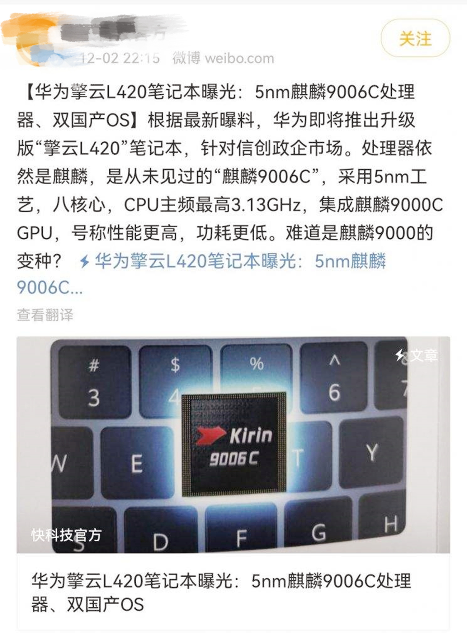
Many people speculate that Huawei may have broken through the chip blockade of Eagle Sauce , because recently Huawei's new products use a Kirin chip that has never been seen before. This chip is called Kirin 9006 .
What makes many people wonder is how this chip was made? We must know that the current blockade of Huawei by Yingjiang has not relaxed at all. Who is so bold and antagonistic to Yingjiang?

In fact, after Eagle Sauce gave Huawei an ultimatum, Huawei, which was unwilling to give in, could only ask TSMC to produce as many chips as possible for itself at the last moment , so that it could hold on for a while when Eagle Sauce suppressed in the future. time. However, at this time, Huawei encountered a serious problem. At that time, Huawei was developing the Kirin 9006 chip, but this chip had not been thoroughly designed yet, and many structures of the chip needed to be perfected, and it had not yet reached the standard for mass production.
But at this time, Huawei knows that if the chip cannot be mass-produced in a short period of time, then this chip will probably stay on the drawing forever, and there will never be a way to be manufactured . This situation is completely unacceptable for Huawei. Huawei has spent a lot of money to develop this chip. If this chip fails at this time , it means that all of Huawei's early investment will be in vain and become meaningless . This will make Huawei, which is already struggling to make a profit this year, even more cramped in the capital chain. So at this time Huawei made a major decision.
Huawei's idea is that since the overall framework of the chip has been laid out, it is better to build the chip first , so that the chip will not be completely stuck on the drawing and there is no way to mass produce it. As for the flaws and deficiencies in the chip design process, Huawei can make up and improve in the future, so that this chip will finally have the strength to carry .
In fact, this is a very risky decision.
First of all, Huawei does not know whether there are loopholes in the design of this chip . Because this chip has not been officially taped out and has not undergone performance testing, Huawei does not know whether there are design flaws in the design of this chip. At this time, it is a very risky decision for Huawei to mass-produce this chip . Because once discovered in the later stage, this chip has design flaws , it is very likely that this chip can not be put into practical applications in the end, which will be a huge loss for Huawei .
Secondly, whether Huawei has the technical strength to perfect these semi-finished chips and finally apply them to the use of products , these are questions that have to be considered. However, in the end, in order to be able to win more capital for the turnaround , Huawei resolutely put this chip into mass production.
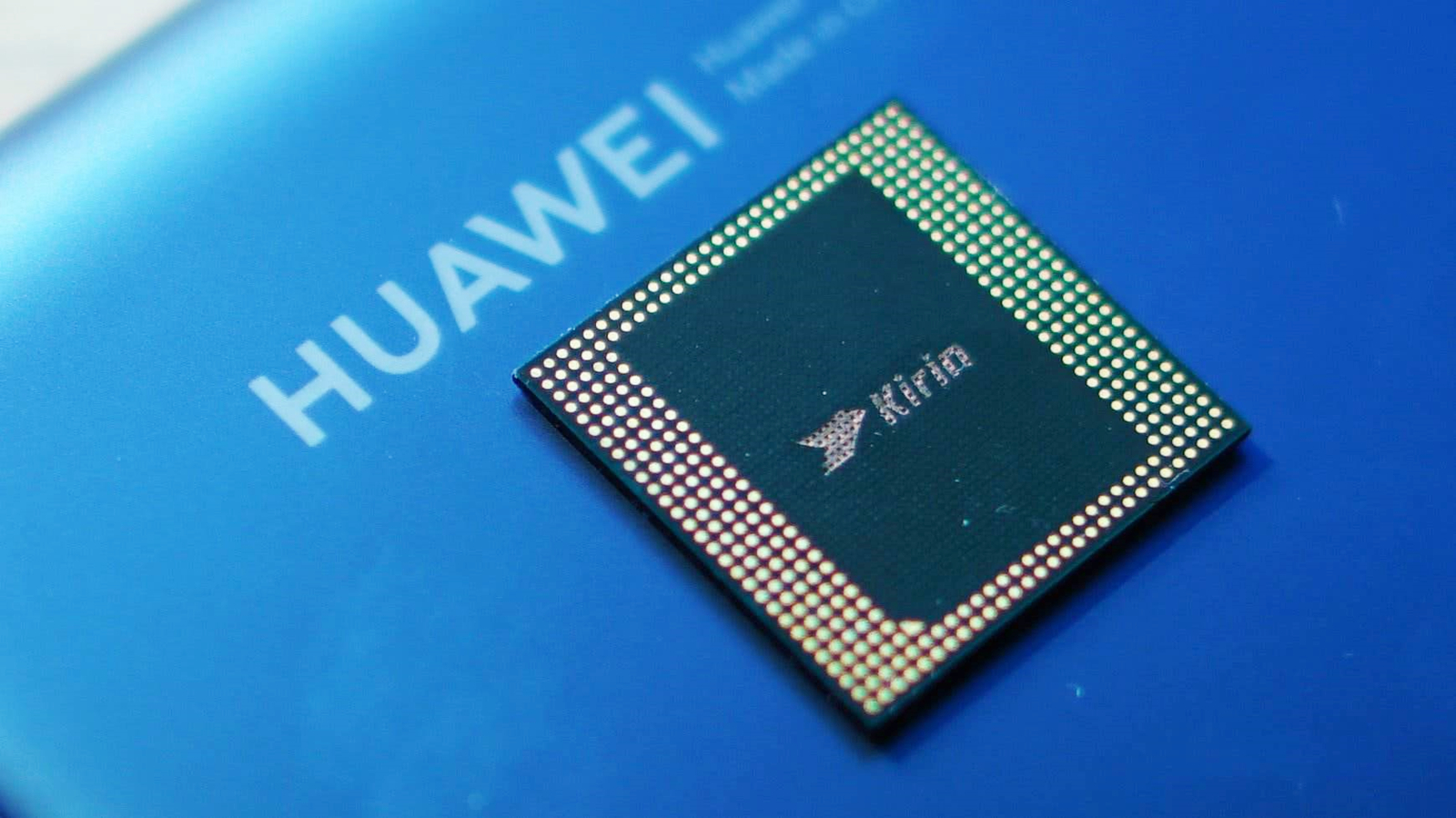
At present, Huawei's latest laptop "Qingyun L420" has begun to carry the low-profile version of the Kirin 9006C of this chip. According to user feedback, this laptop is equipped with Huawei's latest chip, which is superior in performance, fluency, and power consumption. The performance is very good . The advent of the Kirin 9006 caught Eagle-chan by surprise. No one thought that a few months later, Huawei could actually pull out a hole card at this time . It seems that Eagle-chan's desire to defeat Huawei in one fell swoop was completely shattered .
Huawei's foresight has given itself more capital to turn around when fighting against Yingjiang's suppression. Of course, these can only help Huawei persist for a longer time. In the future, if Huawei wants to go more smoothly, it still has to achieve technological breakthroughs. Therefore, we must expect Huawei to make more efforts.
5nm Kirin 9006C chip came out, Huawei once again demonstrated its own strength
Unexpectedly, Huawei still has a hole card! 5nm chip came out, Huawei successfully turned over
5nm Kirin 9006C chip comes out, Huawei successfully breaks through again
2022-05-04 18:58 HKT
Many people speculate that Huawei may have broken through the chip blockade of Eagle Sauce , because recently Huawei's new products use a Kirin chip that has never been seen before. This chip is called Kirin 9006 .
What makes many people wonder is how this chip was made? We must know that the current blockade of Huawei by Yingjiang has not relaxed at all. Who is so bold and antagonistic to Yingjiang?
Huawei's precautions
In fact, everyone has misunderstood that although this chip has just come out, but these chips are not just out of the library, but from Huawei's inventory. This Kirin 9006 chip still uses TSMC technology, and this chip is still the top 5nm process . In terms of structure and performance, Kirin 9006 series chips and Huawei's Kirin 9000 belong to the same brothers , and the similarity between the two is very high in these aspects.
In fact, after Eagle Sauce gave Huawei an ultimatum, Huawei, which was unwilling to give in, could only ask TSMC to produce as many chips as possible for itself at the last moment , so that it could hold on for a while when Eagle Sauce suppressed in the future. time. However, at this time, Huawei encountered a serious problem. At that time, Huawei was developing the Kirin 9006 chip, but this chip had not been thoroughly designed yet, and many structures of the chip needed to be perfected, and it had not yet reached the standard for mass production.
But at this time, Huawei knows that if the chip cannot be mass-produced in a short period of time, then this chip will probably stay on the drawing forever, and there will never be a way to be manufactured . This situation is completely unacceptable for Huawei. Huawei has spent a lot of money to develop this chip. If this chip fails at this time , it means that all of Huawei's early investment will be in vain and become meaningless . This will make Huawei, which is already struggling to make a profit this year, even more cramped in the capital chain. So at this time Huawei made a major decision.

Risky decision
Huawei's risky decision is to let TSMC directly produce the Kirin 9006 chip according to Huawei's current progress in the design of the Kirin 9006 chip . This decision surprised many people. Because this means that even if the Kirin 9006 chip is mass-produced, the obtained chip cannot be used in the product immediately , because it is basically a semi-finished product, and the design of many parts is not complete.Huawei's idea is that since the overall framework of the chip has been laid out, it is better to build the chip first , so that the chip will not be completely stuck on the drawing and there is no way to mass produce it. As for the flaws and deficiencies in the chip design process, Huawei can make up and improve in the future, so that this chip will finally have the strength to carry .

In fact, this is a very risky decision.
First of all, Huawei does not know whether there are loopholes in the design of this chip . Because this chip has not been officially taped out and has not undergone performance testing, Huawei does not know whether there are design flaws in the design of this chip. At this time, it is a very risky decision for Huawei to mass-produce this chip . Because once discovered in the later stage, this chip has design flaws , it is very likely that this chip can not be put into practical applications in the end, which will be a huge loss for Huawei .
Secondly, whether Huawei has the technical strength to perfect these semi-finished chips and finally apply them to the use of products , these are questions that have to be considered. However, in the end, in order to be able to win more capital for the turnaround , Huawei resolutely put this chip into mass production.
Huawei ushered in new opportunities
Facts have proved that Huawei's decision is correct. After several months of hard work, Huawei has relied on its strong technical strength to perfect all of these Kirin 9006 chips . At present, these chips can already be used in products. Through performance testing, Kirin 9006 is superior to Huawei's previous flagship Kirin 9000 in all aspects . It can be seen that Kirin 9006 may help Huawei achieve a new round of technological breakthroughs in the future.
At present, Huawei's latest laptop "Qingyun L420" has begun to carry the low-profile version of the Kirin 9006C of this chip. According to user feedback, this laptop is equipped with Huawei's latest chip, which is superior in performance, fluency, and power consumption. The performance is very good . The advent of the Kirin 9006 caught Eagle-chan by surprise. No one thought that a few months later, Huawei could actually pull out a hole card at this time . It seems that Eagle-chan's desire to defeat Huawei in one fell swoop was completely shattered .
Huawei's foresight has given itself more capital to turn around when fighting against Yingjiang's suppression. Of course, these can only help Huawei persist for a longer time. In the future, if Huawei wants to go more smoothly, it still has to achieve technological breakthroughs. Therefore, we must expect Huawei to make more efforts.
5nm Kirin 9006C chip came out, Huawei once again demonstrated its own strength
Unexpectedly, Huawei still has a hole card! 5nm chip came out, Huawei successfully turned over
- Status
- Not open for further replies.
