They are definitely not starting from zero, that is why ASML do not want export controls because the best way to keep a competitor down is to sell a full complete product so a determined competitor with deep pockets do not spend time and money developing their own.

You are using an out of date browser. It may not display this or other websites correctly.
You should upgrade or use an alternative browser.
You should upgrade or use an alternative browser.
Chinese semiconductor industry
- Thread starter Hendrik_2000
- Start date
- Status
- Not open for further replies.
Shanghai-based Fudan University releases a concept Computing-In-Memory AI chip
A Chinese team from Fudan University in Shanghai proposed COMB-MCM, a Computing-In-Memory (CIM) AI chip at ISSCC 2022, a global solid-state circuits forum known as the "Chip Olympics", according to Fudan University’s Academy for Engineering & Technology website.
This research paper was written by Doctorate student Zhu Haozhe and two other graduate students. They intend to avoid the calculation errors of analog computing circuits and uses multi-chiplet integration to achieve the scalability of computing power after tape-out while keeping the performance and energy efficiency of the "non-von-Neumann" architecture of CIM.
The Fudan University information shows that this chip is manufactured in 65nm and 28nm processes respectively. The feasibility of the solution is verified by the MCM system of 2.5D IC packaging under the 65nm process, and better performance is achieved under the 28nm process.
The Fudan team said the CIM architecture can eliminate unnecessary data movement by integrating the data memory and the computing units, and breaking the von Neumann bottleneck caused by separated CPUs and memory.
Fudan University has mainly carried out technological exploration and innovations. Architecturally, an SRAM-based computing-on-memory-Boundary (COMB) architecture is proposed to further reduce the data movement and system power consumption.
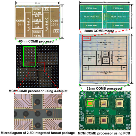
At the system level, it builds a Multi-Chiplet-Module (MCM) to support AI tasks of different complexity. By configuring the number of chiplets, the computing and memory requirements can be increased proportionally.
This technology exhibits ultra-high energy efficiency in AI applications that require intensive memory access and is considered a crucial technology for next-generation AI chips.
Starting in 1954, ISSCC (International Solid-State Circuits Conference) is the foremost global forum for the presentation of advances in solid-state circuits and systems-on-a-chip, according to its website. The Conference offers a unique opportunity for engineers working at the cutting edge of IC design and application to maintain technical currency and to network with leading.
A Chinese team from Fudan University in Shanghai proposed COMB-MCM, a Computing-In-Memory (CIM) AI chip at ISSCC 2022, a global solid-state circuits forum known as the "Chip Olympics", according to Fudan University’s Academy for Engineering & Technology website.
This research paper was written by Doctorate student Zhu Haozhe and two other graduate students. They intend to avoid the calculation errors of analog computing circuits and uses multi-chiplet integration to achieve the scalability of computing power after tape-out while keeping the performance and energy efficiency of the "non-von-Neumann" architecture of CIM.
The Fudan University information shows that this chip is manufactured in 65nm and 28nm processes respectively. The feasibility of the solution is verified by the MCM system of 2.5D IC packaging under the 65nm process, and better performance is achieved under the 28nm process.
The Fudan team said the CIM architecture can eliminate unnecessary data movement by integrating the data memory and the computing units, and breaking the von Neumann bottleneck caused by separated CPUs and memory.
Fudan University has mainly carried out technological exploration and innovations. Architecturally, an SRAM-based computing-on-memory-Boundary (COMB) architecture is proposed to further reduce the data movement and system power consumption.
At the system level, it builds a Multi-Chiplet-Module (MCM) to support AI tasks of different complexity. By configuring the number of chiplets, the computing and memory requirements can be increased proportionally.
This technology exhibits ultra-high energy efficiency in AI applications that require intensive memory access and is considered a crucial technology for next-generation AI chips.
Starting in 1954, ISSCC (International Solid-State Circuits Conference) is the foremost global forum for the presentation of advances in solid-state circuits and systems-on-a-chip, according to its website. The Conference offers a unique opportunity for engineers working at the cutting edge of IC design and application to maintain technical currency and to network with leading.
Suzhou Crystal TestIn 2019, Suzhou Crystal Test was established in Suzhou Industrial Park. It adopts the business model of "AllInHouse" to provide semiconductor test interface services, and helps customers to quickly innovate in the ever-changing semiconductor industry to create a win-win situation. The semiconductor test interface products provided by Suzhou Crystal Test include wafer-level test probe cards, chip test substrates, and high-level printed circuit boards for semiconductor testing. With the independent and controllable probe patent technology, we have launched a complete and diverse range of probe needles equipped with various high-speed, high-frequency, and high-current probe cards to meet the semiconductor testing needs of all terminal application markets.


- IC size is shrinking
- Bump Pitch keeps shrinking
- IC complexity improvement
- Signal transmission speed increased

When IC Bump miniaturization will face the challenges of two technologies, one is tiny aperture, the other is tiny line width / spacing,
At present , the technology of crystal testing has reached 20um for micro-pitch and 20um for fine lines .
tiny aperture
The lithography process is used to replace the mechanical process, and the thin-film technology is combined to produce tiny apertures.
Therefore , Crystal Test replaced the 2D structure with 2.5D , and established related patents for the structure and process.
Micro line width / spacing
Through the miniaturization of L/S , it will provide more space for wiring, in addition to reducing the number of layers of Layout , it can also provide Multi-DUT test design,
In addition, the signal transmission path is shortened, which will help to improve the signal quality. Crystal Test has experience in mass production of pitch 50um, except the aperture is set to 25um ,
L/S is set to 20um/20um , and this test solution can already correspond to the test of the wafer 10nm process level.
2021 New Probe Cards
Fine pitch/fine lines
In recent years, packaging technology has continued to evolve. From Wire Bond to 3D IC , the miniaturization of IC Bump will become an inevitable trend. The advancement of packaging technology also indirectly affects the development of the following technologies.- IC size is shrinking
- Bump Pitch keeps shrinking
- IC complexity improvement
- Signal transmission speed increased
When IC Bump miniaturization will face the challenges of two technologies, one is tiny aperture, the other is tiny line width / spacing,
At present , the technology of crystal testing has reached 20um for micro-pitch and 20um for fine lines .
tiny aperture
The lithography process is used to replace the mechanical process, and the thin-film technology is combined to produce tiny apertures.
Therefore , Crystal Test replaced the 2D structure with 2.5D , and established related patents for the structure and process.
Micro line width / spacing
Through the miniaturization of L/S , it will provide more space for wiring, in addition to reducing the number of layers of Layout , it can also provide Multi-DUT test design,
In addition, the signal transmission path is shortened, which will help to improve the signal quality. Crystal Test has experience in mass production of pitch 50um, except the aperture is set to 25um ,
L/S is set to 20um/20um , and this test solution can already correspond to the test of the wafer 10nm process level.
Alibaba DAMO academy released something similar in December.Shanghai-based Fudan University releases a concept Computing-In-Memory AI chip
A Chinese team from Fudan University in Shanghai proposed COMB-MCM, a Computing-In-Memory (CIM) AI chip at ISSCC 2022, a global solid-state circuits forum known as the "Chip Olympics", according to Fudan University’s Academy for Engineering & Technology website.
This research paper was written by Doctorate student Zhu Haozhe and two other graduate students. They intend to avoid the calculation errors of analog computing circuits and uses multi-chiplet integration to achieve the scalability of computing power after tape-out while keeping the performance and energy efficiency of the "non-von-Neumann" architecture of CIM.
The Fudan University information shows that this chip is manufactured in 65nm and 28nm processes respectively. The feasibility of the solution is verified by the MCM system of 2.5D IC packaging under the 65nm process, and better performance is achieved under the 28nm process.
The Fudan team said the CIM architecture can eliminate unnecessary data movement by integrating the data memory and the computing units, and breaking the von Neumann bottleneck caused by separated CPUs and memory.
Fudan University has mainly carried out technological exploration and innovations. Architecturally, an SRAM-based computing-on-memory-Boundary (COMB) architecture is proposed to further reduce the data movement and system power consumption.
At the system level, it builds a Multi-Chiplet-Module (MCM) to support AI tasks of different complexity. By configuring the number of chiplets, the computing and memory requirements can be increased proportionally.
This technology exhibits ultra-high energy efficiency in AI applications that require intensive memory access and is considered a crucial technology for next-generation AI chips.
Starting in 1954, ISSCC (International Solid-State Circuits Conference) is the foremost global forum for the presentation of advances in solid-state circuits and systems-on-a-chip, according to its website. The Conference offers a unique opportunity for engineers working at the cutting edge of IC design and application to maintain technical currency and to network with leading.
近日,阿里巴巴达摩院宣布已成功研发存算一体芯片。据介绍,达摩院介绍,该存算一体芯片集成了多项创新技术,是全球首款使用“混合键合3D堆叠技术”实现存算一体的AI芯片,可突破冯·诺依曼架构的性能瓶颈,满足人工智能等场景对高带宽、高容量内存和极致算力的需求。在特定AI场景中,该芯片性能提升10倍以上,能效比提升高达300倍以上。
DAMO was also presenting it in the same ISSCC. Found their session in this PDF:
184QPS/W 64Mb/mm 2 3D Logic-to-DRAM Hybrid Bonding with Process-Near-Memory Engine for Recommendation System
D. Niu1, S. Li1 , Y. Wang1, W. Han1, Z. Zhang2, Y. Guan2, T. Guan3, F. Sun1 , F. Xue1, L. Duan1, Y. Fang1,
H. Zheng1, X. Jiang4 , S. Wang4, F. Zuo 4 , Y. Wang 4, B. Yu4, Q. Ren4, Y. Xie 1
1 Alibaba DAMO Academy, Sunnyvale, CA
2 Alibaba DAMO Academy, Beijing, China
3 Alibaba DAMO Academy, Shanghai, China
4 UniIC, Xian, China
US commerce secretary has to "essentially shut down" SMIC if China doesn't co-operate on sanctioning Russia. How realistic are these threats today? The main pressure points would be litography machines and software tools. I know China has their own companies in both areas but would they be able to substitute Western alternatives if push came to shove? (Obviously there is no Chinese equivalent to ASML so I am not talking about leading-edge tech, but trailing edge stuff).
They played their cards in grade war already. They cant do further damage.US commerce secretary has to "essentially shut down" SMIC if China doesn't co-operate on sanctioning Russia. How realistic are these threats today? The main pressure points would be litography machines and software tools. I know China has their own companies in both areas but would they be able to substitute Western alternatives if push came to shove? (Obviously there is no Chinese equivalent to ASML so I am not talking about leading-edge tech, but trailing edge stuff).
Didn't they already exercise their nuclear option by cutting off ASML?US commerce secretary has to "essentially shut down" SMIC if China doesn't co-operate on sanctioning Russia. How realistic are these threats today? The main pressure points would be litography machines and software tools. I know China has their own companies in both areas but would they be able to substitute Western alternatives if push came to shove? (Obviously there is no Chinese equivalent to ASML so I am not talking about leading-edge tech, but trailing edge stuff).
@TK3600 Yup they keep beating a dead horse, PETA should investigate...lolThey played their cards in grade war already. They cant do further damage.
- Status
- Not open for further replies.