Chinese semiconductor industry

Status
Not open for further replies.

supersnoop

Major
Registered Member
EUV is a little overrated.
Intel does not use EUV in anything shipping right now.
Yes they are a bit behind TSMC, but it is nothing like 10 years behind or anything like that.
So you do not have to be on EUV to achieve great performance.

Of course Chinese organizations will try to skip steps when possible. 3G HSPA/4G FD-LTE was basically skipped for 5G, steam catapults supposedly skipped for EMALS, etc.

But it is not the end all here.
 

horse

Colonel
Registered Member
EUV is a little overrated.

But it is not the end all here.

It's symbolic.

Western dominance of tech, is not be broken here, it is being shattered.

The west is still ahead in a lot of tech, maybe such as IC, pharmaceutics, etc ...

However, the Chinese, basically are at the leading edge of a lot tech as well.

For someone like me, a lay person, what seems to be the breakthrough here for the Chinese is very significant.

They said that only truly advanced industrial countries can build something like a fighter aircraft, which China does, even built stealth aircraft. The same goes for the nuclear industry and space exploration.

The IC industry is like the same, IC is that intricate.

When a Chinese EUV appears, that means China is the only country in the world that has a full home made IC industry. That is also at the leading edge. That speaks volumes about Chinese tech.

Then we still have the Americans trying to sanction Chinese tech, left right and center.

:D
 

ZeEa5KPul

Colonel
Registered Member
It looks like the R&D on SSMB will principally be carried out at the new HEP Synchrotron which is under construction in Beijing.
All the equipment required for the SSMB Research should be installed by early 2022.
This Synchroton in Beijing will be where the first Prototype SSMB Light Source Equipment will be located.
The Chinese Academy of Sciences will be taking charge of the R&D on SSMB.
Tsinghua Uni has a separate collaboration with other countries on SSMB Research but in light of the New Technology Cold War, it is doubtful this collaboration will continue.
HEPS is scheduled to be completed at the end of 2025; I don't see how it can be used to test SSMB in the near term
Please, Log in or Register to view URLs content!
Could you be a little more specific on what's required? The schedule shows some components being installed in 2022, but the earliest commissioning happens in 2023. Furthermore, HEPS is a scientific instrument, it won't be used industrially for EUV lithography. HEPS might certainly be used to validate and test the SSMB phenomenon, and even to develop candidate EUV optics, but it won't be used to make chips. A dedicated synchrotron will have to be built, which I believe is what the Tsinghua project is. I believe that's what we should be keeping our eye on - it seems a much simpler device for the specific EUVL purpose, not a much more complex general-purpose experimental device.

This lends weight to my initial thoughts that SSMB is more for the 2030 timeframe (perhaps a bit earlier, 2027+ if things go well). Near term (around 2024-2025), I believe LPP is a more viable candidate. I believe China will at least have one generation of LPP EUV before it transitions to synchrotron light sources.
 

ansy1968

Brigadier
Registered Member
It looks like the R&D on SSMB will principally be carried out at the new HEP Synchrotron which is under construction in Beijing.
All the equipment required for the SSMB Research should be installed by early 2022.
This Synchroton in Beijing will be where the first Prototype SSMB Light Source Equipment will be located.
The Chinese Academy of Sciences will be taking charge of the R&D on SSMB.
Tsinghua Uni has a separate collaboration with other countries on SSMB Research but in light of the New Technology Cold War, it is doubtful this collaboration will continue.
@WTAN Sir @Oldschool had been following your post and he sent this for your perusal.

Oldschool

Junior Member​

Registered Member
Today at 8:33 AMNew
A nice video on Beijing synchrotron multidisciplinary project. It can generate X ray, EUV light

Please, Log in or Register to view URLs content!

高能同步辐射光源是中国“十三五”期间优先建设的大科学装置。装置于2025年底验收并投入运行,是中国第一台高能同步辐射光源,也是世界上最亮的第四代同步辐射光源。2019年5月,高能同步辐射光源在北京科技周上亮相。2021年6月28日,由国家发展改革委立项支持、中国科学院高能物理研究所承担建设的高能同步辐射光源(HEPS)[L1] 首台科研设备安装。
baike.baidu.com
baike.baidu.com

Like Quote Reply
Report


high energy synchrotron radiation source​

broadcastedit
Please, Log in or Register to view URLs content!
upload video

The High-Energy Synchrotron Radiation Light Source is a major scientific installation prioritized during China's "Thirteenth Five-Year Plan" period. The device will be accepted and put into operation at the end of 2025. It is the first high-energy synchrotron radiation source in China and the brightest fourth-generation synchrotron radiation source in the world.
In May 2019, the High Energy Synchrotron Radiation Light Source was unveiled at the Beijing Science and Technology Week. [1]
On June 28, 2021, the first scientific research equipment of the High Energy Synchrotron Light Source (HEPS) [L1], which was supported by the National Development and Reform Commission and undertaken by the Institute of High Energy Physics, Chinese Academy of Sciences, was installed. [5]


Chinese namehigh energy synchrotron radiation sourceforeign nameHighEnergyPhotonSource [2] Approval timeDecember 15, 2017Construction period6.5 years

content​

  1. 1
    Please, Log in or Register to view URLs content!
  2. 2
    Please, Log in or Register to view URLs content!
  3. Please, Log in or Register to view URLs content!
  4. Please, Log in or Register to view URLs content!
  5. 3
    Please, Log in or Register to view URLs content!

R & D process​

edit broadcast
In April 2016, the prefabricated research and key technology research project of the High Energy Synchrotron Radiation Source (HEPS) project - High Energy Synchrotron Radiation Source Verification Facility (HEPS-TF) was officially launched. HEPS-TF is China's national major scientific and technological infrastructure "Twelfth Five-Year" construction project. [3]
On December 15, 2017, the High Energy Synchrotron Light Source (HEPS) project proposal was officially approved by the National Development and Reform Commission of China. The project construction period is 6.5 years. [3]
On January 31, 2019, the High Energy Photon Source Test Facility (HEPS-TF) passed the project acceptance. [2]
In May 2019, at the Beijing Science and Technology Week, the ring-shaped "high-energy synchrotron radiation light source" was unveiled, arousing the onlookers of the audience.
In mid-2019, the "High-Energy Synchrotron Radiation Light Source" device is expected to start construction in the northern core area of Huairou Science City. It will be accepted and put into operation by the end of 2025. It is the first high-energy synchrotron radiation source in China and the brightest fourth-generation synchrotron in the world. radiation source. [1]
On June 29, 2019, China's first high-energy synchrotron radiation light source started construction in Huairou, Beijing. [4]
On June 28, 2021, the first scientific research equipment of the High-Energy Synchrotron Light Source (HEPS) [L1], which was supported by the National Development and Reform Commission and undertaken by the Institute of High Energy Physics, Chinese Academy of Sciences, was installed, marking the official entry of this large scientific device into the equipment. installation phase. [5]
Please, Log in or Register to view URLs content!
high energy synchrotron radiation source

Construction​

edit broadcast

architectural design​

The entire building is shaped like a magnifying glass, implying that it is a tool for exploring the microscopic world. The building mainly includes accelerators, beamlines and experimental stations. The high-flux X-rays produced in the circular accelerator travel through the "channel" to the experimental station. After the construction of the device is completed, it can accommodate no less than 90 experimental stations at most, and can do "physical examinations" for different samples. The design life of the device is 30 years, and it will continue to be remodeled after it is completed. It is expected to have a working life of 50 years. [1]

Construction unit​

The high-energy synchrotron radiation source is constructed by the
Please, Log in or Register to view URLs content!
as a legal entity in Huairou District, Beijing. The project investment is funded by the Chinese state and Beijing.

Engineering goals​

edit broadcast
The energy of the storage ring reaches 6 gigaelectron volts, the emissivity is less than 0.06 nanometer radian, the capacity of high-performance beamline stations is not less than 90, and the X-rays with the energy of 300 kiloelectron volts are provided. Time resolution and millielectron volt energy resolution. [3]
Please, Log in or Register to view URLs content!
high energy synchrotron radiation source

Entry Atlas
 

antiterror13

Brigadier
It's symbolic.

Western dominance of tech, is not be broken here, it is being shattered.

The west is still ahead in a lot of tech, maybe such as IC, pharmaceutics, etc ...

However, the Chinese, basically are at the leading edge of a lot tech as well.

For someone like me, a lay person, what seems to be the breakthrough here for the Chinese is very significant.

They said that only truly advanced industrial countries can build something like a fighter aircraft, which China does, even built stealth aircraft. The same goes for the nuclear industry and space exploration.

The IC industry is like the same, IC is that intricate.

When a Chinese EUV appears, that means China is the only country in the world that has a full home made IC industry. That is also at the leading edge. That speaks volumes about Chinese tech.

Then we still have the Americans trying to sanction Chinese tech, left right and center.

:D

Well ....... in near future, it could be reverse .. China sanction American tech companies ;)

Karma does work, whether you believe it or not

Covid ... you know what happenend
Hongkong ... 6 Jan and whats happening now in Canada, etc
etc
etc
 

GumNaam

New Member
Registered Member
Well ....... in near future, it could be reverse .. China sanction American tech companies ;)

Karma does work, whether you believe it or not

Covid ... you know what happenend
Hongkong ... 6 Jan and whats happening now in Canada, etc
etc
etc
China can sanction not just american tech companies but all companies.
 

foofy

Junior Member
Registered Member
HEPS is scheduled to be completed at the end of 2025; I don't see how it can be used to test SSMB in the near term
Please, Log in or Register to view URLs content!
Could you be a little more specific on what's required? The schedule shows some components being installed in 2022, but the earliest commissioning happens in 2023. Furthermore, HEPS is a scientific instrument, it won't be used industrially for EUV lithography. HEPS might certainly be used to validate and test the SSMB phenomenon, and even to develop candidate EUV optics, but it won't be used to make chips. A dedicated synchrotron will have to be built, which I believe is what the Tsinghua project is. I believe that's what we should be keeping our eye on - it seems a much simpler device for the specific EUVL purpose, not a much more complex general-purpose experimental device.

This lends weight to my initial thoughts that SSMB is more for the 2030 timeframe (perhaps a bit earlier, 2027+ if things go well). Near term (around 2024-2025), I believe LPP is a more viable candidate. I believe China will at least have one generation of LPP EUV before it transitions to synchrotron light sources.
Shenzhen is constructing a FEL.
 

Strangelove

Colonel
Registered Member
Please, Log in or Register to view URLs content!

2,810 companies, including big names, drive semiconductor sector's fast growth

Chinese carmakers, cloud computing companies and smartphone vendors are branching out into chip design as processors developed in-house become key to differentiating their products and services from those of rivals.

The trend follows a prolonged global chip supply crunch and highlights the importance of chips to both economic recovery from sporadic outbreaks of COVID-19 and future economic growth.

Chinese companies are leveraging the strategic opportunities brought by artificial intelligence, the internet of things and self-driving vehicles to grow their strength in the semiconductor sector.

Gan Jiayue, CEO of Chinese automobile company Geely Holding Group, for instance, said in February that the company is scheduled to produce the country's first automotive 7-nanometer chip in the third quarter of this year.

The chip, called SE1000, is designed by Siengine, a chip joint venture established by the chip company Arm and EcarX, which is owned by Geely Holding Group.

Gan said the chip, designed to support smart onboard features, will be first installed in one of Geely's most popular models, and the company also has plans to produce autonomous driving chips and onboard central processing units in the future.

Prior, another Chinese carmaker Great Wall Motors said in December that it had led a financing round for Chinese chip company Synlight Crystal.

Great Wall Motors did not disclose the specific amount of its investment but said it will help accelerate Synlight Crystal's business development in electric vehicles, thus facilitating the commercialization of silicon carbide material and chips.

The prolonged chip supply crunch has affected more than 169 industries in the world to some extent in 2021, ranging from automobiles, steel products, smartphones and air conditioning, according to a report from Goldman Sachs.

Miao Wei, former minister of industry and information technology, said a lesson from the global chip shortages is that China needs a strong indigenous auto chip industry.

"We are in an age where software defines cars, and cars need central processing units and operating systems. So, we should plan in advance," Miao said last year at a Chinese auto show.

In addition to carmakers, Chinese cloud computing players are jumping on the chip bandwagon. So have the "big three" Chinese internet giants, which have placed bets on the semiconductor sector, attributing their moves to their need to meet their own growing demand for chips.

For instance, Tencent Holdings Ltd's cloud computing business in November unveiled three chips developed in-house. The company said one of the chips is already taped out.

Dowson Tong, senior executive vice-president of Tencent, said the company's investments in chips are driven by the need to solve problems in its sprawling businesses. For instance, video technologies account for an increasingly larger part of its business that spans medical care, education and livestreaming. These business lines need very large amount of computing resources. So, the company developed a tailor-made chip that can support video transcoding more efficiently.

For its part, Alibaba Cloud, the cloud computing business of Alibaba Group Holding Ltd, unveiled a new self-designed server chip based on advanced 5-nanometer technology in October, two years after it unveiled its first chip built in-house in 2019.

Alibaba Cloud said the latest chip is based on micro-architecture provided by SoftBank Group Corp-owned Arm Ltd, and the silicon will be put into use at its own data centers in the "near future" and will not be sold commercially, at least for now.

Jeff Zhang, president of Alibaba Cloud Intelligence and head of Alibaba's research arm Damo Academy, said: "Customizing our own server chips is consistent with our ongoing efforts toward boosting our computing capabilities with better performance and improved energy efficiency. We plan to use the chips to support current and future businesses across the Alibaba Group ecosystem."

Chinese internet heavyweight ByteDance, owner of the popular short-video app TikTok, also said in December that it is marching into the cloud computing business, and its first self-designed AI chip would soon enter trial production.

Yang Zhenyuan, vice-president of ByteDance, said the whole internet world is seeing fundamental changes and internet companies are faster to see the new emerging demand than traditional semiconductor companies.

"We will beef up investments in areas and technologies that change fast in hardware," Yang said, adding that internet companies devote resources to self-designed chips because they want to have advantages in competition and to seek cost-effective performance.

Such a desire has also spurred many Chinese phone makers to invest in semiconductors. Oppo, for instance, unveiled its first self-developed chip in December, joining the ranks of international peers such as Apple and domestic counterparts such as Huawei and Xiaomi to have more control over its own semiconductor design.

Oppo's chip-MariSilicon X-is a neural processing unit, or NPU, which can assist in enhancing images by leveraging the power of artificial intelligence. MariSilicon X is expected to sharpen Oppo's technological prowess as competition in the global smartphone market intensifies.

Chen Mingyong, founder and CEO of Oppo, said MariSilicon X was unveiled after three years of research and development. Built on 6-nanometer process technology, it is a dedicated imaging NPU designed to meet growing consumer demand for better mobile imaging technologies.

Chen further said the experience of developing in-house chips is destined to be bumpy. The chip's name tells a story. Mariana is the deepest trench in the world, implying the difficulty of developing in-house chips. But MariSilicon X is just the first step and the company will continue to invest resources in chip R&D with a team of thousands, Chen said.

Fu Liang, an independent telecom analyst, said the move is of long-term significance for Oppo and will increase its competence amid the cutthroat competition in the smartphone sector, as underlying chip technologies are widely seen as crucial for hardware companies.

The chip industry, he said, has always been capital- and technology-intensive. The investment by domestic mobile phone companies in this field is just a starting point.

China has seen an upsurge in chip design companies in recent years. Wei Shaojun, chairman of integrated circuit design branch of the China Semiconductor Industry Association, said China has more than 2,810 chip design firms as of 2021, marking a 27 percent year-on-year surge, and 2021 was the second year to see double-digit growth.

Huang Qing, China managing director of Walden International, a US venture capital company focused on cross-border investments, said earlier: "As the US government moves to tighten export of key technologies including premium processors to Chinese companies, China is facing an unprecedented opportunity to build up its chip capabilities."

Given US export controls, Chinese firms have begun to feel an urgent need to work with domestic semiconductor companies, and they also devote more resources to self-designed chips, Huang said. "By serving such tech giants, Chinese chip companies have an unprecedented opportunity to grow into global players."

Pan Jianyue, founding partner of SummitView Capital, a Chinese investment company, said there are still many weak points in China's chip industry, including raw materials, manufacturing equipment, chip design tools, and the lack of crucial intellectual properties.

However, the wider use of AI as well as the increasing popularity of internet of things applications and self-driving vehicles will spawn a new wave of computing brands and chip companies, analysts and investors said.

Shen Ziyu, CEO of Siengine, the chip joint venture of Geely and Arm, said Huawei and Apple are shining examples in the smartphone industry as they have allocated heavy resources for self-designed chips.

Similarly, by emulating peers in the automobile and other industries, companies should develop their own products that are globally competitive and popular, Shen said.
 

tokenanalyst

Brigadier
Registered Member

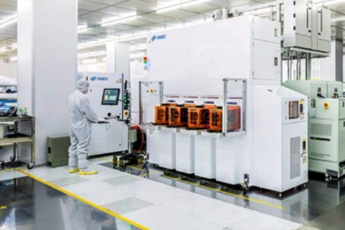
Newly signed orders have increased significantly, and China Micro's(AMEC) 2021 net profit will increase by 105% year-on-year​


16456073224992.png


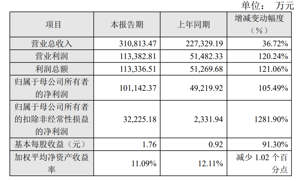
Jiwei.com news, on February 23, Zhongwei announced that in 2021, its operating income will be 3.108 billion yuan, a year-on-year increase of 36.72%; the net profit attributable to the parent is 1.011 billion yuan, a year-on-year increase of 105.49%; basic earnings per share are 1.76 yuan.

16456073336747.png


As for the reasons for the changes in performance, Zhongwei said that the main reasons are: Benefiting from the development of the semiconductor equipment market and the company's product competitiveness, the revenue of etching equipment in 2021 will be 2.004 billion yuan, an increase of about 55.44% over 2020, and the gross profit margin will reach 44.31% ; Due to downstream market reasons and the newly signed Mini-LED MOCVD equipment scale orders this year, the revenue has not yet been confirmed. In 2021, the revenue of MOCVD equipment will be 503 million yuan, an increase of about 1.53% over 2020, but the gross profit margin of MOCVD equipment will reach 33.77%, This is a significant increase from 18.65% in 2020. The company's newly signed orders in 2021 amounted to 4.13 billion yuan, an increase of about 1.96 billion yuan compared with 2020, an increase of about 90.5% year-on-year.

Please, Log in or Register to view URLs content!
 
Status
Not open for further replies.
Top