Chinese semiconductor industry

Status
Not open for further replies.

european_guy

Junior Member
Registered Member
Please, Log in or Register to view URLs content!
This new open source linux used large scale AI model system being developed by BAAI will pull in all the major chip producers in China as well as Huawei & Inspur.

It's getting help from Baidu PaddlePaddle, Inspur AI Station & China mobile Jiutian as well as Kunlunxin and Tianshu. Looks like a national effort in AI that will also make itself available to international developers.
Talks about using domestic CPU also

And Biren too

Please, Log in or Register to view URLs content!

I tried to understand what kind of platform is:

Please, Log in or Register to view URLs content!

But is not very clear to me. It seems a framework, or better, a collection of frameworks to download and train off-the-shelf or custom AI models. An attempt to converge the different Chinese frameworks and AI platforms in a shared one and to foster collaboration among the many Chinese actors in AI. I don't if there is something similar in US.
 

caudaceus

Senior Member
Registered Member
And Biren too

Please, Log in or Register to view URLs content!

I tried to understand what kind of platform is:

Please, Log in or Register to view URLs content!

But is not very clear to me. It seems a framework, or better, a collection of frameworks to download and train off-the-shelf or custom AI models. An attempt to converge the different Chinese frameworks and AI platforms in a shared one and to foster collaboration among the many Chinese actors in AI. I don't if there is something similar in US.
Please, Log in or Register to view URLs content!
 

tphuang

Lieutenant General
Staff member
Super Moderator
VIP Professional
Registered Member
And Biren too

Please, Log in or Register to view URLs content!

I tried to understand what kind of platform is:

Please, Log in or Register to view URLs content!

But is not very clear to me. It seems a framework, or better, a collection of frameworks to download and train off-the-shelf or custom AI models. An attempt to converge the different Chinese frameworks and AI platforms in a shared one and to foster collaboration among the many Chinese actors in AI. I don't if there is something similar in US.
Involves a few more player, looks like CE Cloud is involved here also. They build cloud solution using domestic CPUs
Please, Log in or Register to view URLs content!

Please, Log in or Register to view URLs content!
然后感受一下今天涨幅,C位中国电子云(
Please, Log in or Register to view URLs content!
+10%),
Please, Log in or Register to view URLs content!
(+9.55%),
Please, Log in or Register to view URLs content!
(+4.98%),启元世界(
Please, Log in or Register to view URLs content!
+13.56%)(具体细分领域应用的航天信息表现欠佳),核桃编程是谁?一级市场目前估值最高的编程教育公司,高瓴重仓的。

这几个联合实验室是什么?

-联合中国电子云建立大模型国产算力云平台开放实验室,探索国产CPU的大模型适配部署;

-联合
Please, Log in or Register to view URLs content!
建立大模型开源生态联合实验室,共同推动国产AI硬件底层软件的完善;

-联合
Please, Log in or Register to view URLs content!
研究院建立AI基础模型服务开放实验室,面向行业应用场景的听觉内容分析等领域进行大模型研究与应用;

-联合航天信息建立智慧政企人工智能开放实验室,探索税务、政务领域的模型能力调优、模型研发、算法研究等;

-联合启元世界建立认知决策大模型开放实验室,探索AI NPC、数字人AI等场景的大模型应用;

-联合核桃科技建立国产3D图形化AI编程平台开放实验室,共同开展基于开源体系的国产化编程平台工具研发
Looks like it combines several research labs including the one by China Mobile which we know Biren and several GPU makers joined before. We also know that Inspur has been building its own AI ML/Big data research lab with many domestic GPUs.
This is the news of China Mobile research lab from December
Please, Log in or Register to view URLs content!
发布FlagOpen这个开源算法体系和一站式基础软件平台,意在做中国AI大模型的基础设施和基座
The goal is to be the one stop shop intending to be the foundation of China's AI big model.

FlagOpen配套了六个模块,分别是FlagAI、FlagPerf、FlagEval、FlagData、FlagStudio和FlagBoot:
FlageAI集成了很多主流大模型算法技术,以及多种大模型并行处理和训练加速技术,并支持微调。
FlagAI supports many big model algo
FlagPerf搭建的AI硬件评测体系,支持多种深度学习框架,可及时跟进最新主流模型评测需求,便于AI芯片厂商插入底层支撑工具,且不以排名为核心目标。
FlagPerf supports many deep learning framework
FlagEval是覆盖多个模态领域、包含评测维度的评测工具,首先开放的是近期很火的多模态领域-CLIP系列模型评测工具,支持多语言多任务、开箱即用。
FlagEval supports multi-language and multi-tasking
FlagData数据工具开源项目集成包含清洗、标注、压缩、统计分析等功能在内的多个数据处理工具与算法。此前,智源研究院已经构建了WuDaoCorpora语料库。
FlagData integrates multiple data processing tools and algorithms for cleaning, labeling....
FlagStudio是文生图、文生音乐等艺术创作相关的开源项目集合,集合的算法和模型更贴合中文场景,当前主要提供智源研究院文生图相关能力的应用。
FlagStudio is for art creation
FlagBoot是基于Scala开发的轻量级高并发微服务框架,默认完全异步,且没有宏、隐式转换等晦涩难懂的代码。极少的代码量便于开发者轻易了解背后逻辑,而后进行自定义修改。
Lightweight framework developed on Scala

This to me seems like a national collaborative effort to use all domestic products and get away from Nvidia, CUDA, PyTorch and such.

So if you know how to use any of the ML framework like Baidu PaddlePaddle, you can use this open source platform and take advantage of the cloud resource with domestic CPU/GPUs and algorithms and tools behind that
 
Last edited:

tokenanalyst

Brigadier
Registered Member

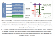
Exploration of next-generation lithography technology: the concept, technology and future of the sixth-generation dual-beam super-resolution.​


Integrated circuits have been developed for more than 60 years, and the pursuit of more powerful chips has led to continuous iterative upgrades of chip manufacturing technology. For a long time, the chip manufacturing method based on ultraviolet light source projection exposure lithography is the only choice for large-scale integrated circuit manufacturing. However, with the entry of extreme ultraviolet lithography machines into production lines and continuous performance optimization, chip manufacturing has entered the 7nm and below nodes. Regarding whether Moore's Law can continue and whether extreme ultraviolet lithography can support future chip demand, the academic and industrial circles have not formed a consensus and a consensus next-generation lithography technology route. Compared with the fifth-generation lithography machine based on extreme ultraviolet projection exposure, this paper proposes the concept of the sixth-generation lithography machine based on dual-beam super-resolution technology, and discusses the sixth-generation lithography machine based on dual-beam super-resolution technology from multiple perspectives The advantages and potential of the technology are discussed, and the difficulties and possible solutions of the technology are also discussed. As an alternative technology route different from the ultraviolet lithography technology route, the dual-beam super-resolution lithography machine technology will most likely lead future chip manufacturing.

1677702416973.png1677702504863.png

8 Conclusion​

The dual-beam super-resolution technology originated from the stimulated radiation microscopic imaging technology pioneered by Professor Stefan Hell in Germany. The core idea of this technology was applied to optical manufacturing. The first realization was the dual-beam super-resolution direct writing lithography technology. In the field of optical manufacturing, limited by the understanding of the optical diffraction limit, there has long been a problem of confusion between line width and line center spacing. Although the early research work of dual-beam super-resolution direct writing lithography technology has confirmed that this method can produce smaller line widths, the line width and line center spacing are obviously not the same thing in the field of lithography. The author's early work on dual-beam super-resolution direct writing lithography not only confirmed that the line width can reach below 10 nm, but more importantly, it confirmed for the first time that the center-to-line spacing can reach about 50 nm. This provides a key basis for the technology to truly break through the diffraction limit and manufacture high-density devices. However, although the author of this paper has first launched a commercial dual-beam super-resolution direct writing lithography equipment in the world, the key point of this direct writing technology is that it cannot be projected and exposed, so it is impossible to apply For industrial chip manufacturing, only proofing can be done at most. In order to improve the manufacturing speed, a multi-focus dual-beam super-resolution direct writing technology based on phase modulation was proposed [
Please, Log in or Register to view URLs content!
], but such methods are still essentially based on direct writing. To catch up with the production speed of projection exposure, the number of multi-focus points will be more than tens of millions to achieve the production speed of GB data per single exposure. However, so far, there is no literature that shows that similar methods can be used to produce uniform and distortion-free multi-focals with a number of more than 10 million, and there is no data that discusses the influence of paraxial optical approximation on the calculation of patterns. Complex high-density pattern decomposition and other related problems. In order to completely solve the problem of speed, this paper proposes a projection-type dual-beam super-resolution lithography machine technology based on yin-yang complementary reticle. In this technology, the negative-yang complementary mask can be produced by the conventional method of etching a chrome-plated metal plate, or by using spatial light modulation to generate surface patterns. For various multi-focus patterns produced by phase modulation, etc., they are all a special case that can be compatible with complementary reticles of Yin and Yang characters, thus realizing the projection-type dual-beam super-resolution lithography machine technology proposed in this paper. Compatible with related technologies. The technology proposed in this paper solves the problem that the existing UV lithography technology must use short-wavelength light sources to achieve nanometer resolution, which can greatly reduce the manufacturing difficulty and cost of high-end lithography machines, and is fully compatible with existing UV lithography machines. technology. Compared with the existing UV lithography machine technology, although the dual-beam super-resolution lithography machine technology has correspondingly increased difficulties in the optical system and photoresist, the analysis in this paper shows that these increased difficulties can be solved in engineering , and its cost will be far less than the cost brought by the use of extreme ultraviolet light source for the development of lithography machine. This points out a new feasible route for the next-generation lithography machine technology that is independent of the UV lithography machine technology route. For developing countries such as China, due to restrictions such as the Wassenaar Agreement, the embargo of high-end lithography machines to China and other countries has become a reality. The new dual-beam super-resolution lithography machine technology is expected to make restricted countries On the premise of a new technical route and greatly reducing the difficulty of development, an independent high-end chip manufacturing production line has been developed.

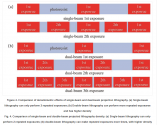
Please, Log in or Register to view URLs content!


xypher

Senior Member
Registered Member
Please, Log in or Register to view URLs content!
Well if I read the FlagAI's description correctly, then it is not similar to ONNX. The latter is essentially just a set of operators, some "unified" format for the deep learning models to which you can convert your TensorFlow\PyTorch\etc. models, just by itself it does not support training of models at all (only through ONNX RunTime which needs PyTorch) and while you can inference models using ONNX, deployment is usually done with specific libraries\frameworks that just use ONNX as a model format - e.g. NVIDIA's TensorRT, Qualcomm's SNPE or QNN, etc.

FlagAI seems to be more of a high-level wrapper library to make training and deployment of large-scale models easier. Something like PyTorch Lightning for training and TensorFlow Lite for deployment are probably closer comparisons.
 
Last edited:

FairAndUnbiased

Brigadier
Registered Member

Exploration of next-generation lithography technology: the concept, technology and future of the sixth-generation dual-beam super-resolution.​


Integrated circuits have been developed for more than 60 years, and the pursuit of more powerful chips has led to continuous iterative upgrades of chip manufacturing technology. For a long time, the chip manufacturing method based on ultraviolet light source projection exposure lithography is the only choice for large-scale integrated circuit manufacturing. However, with the entry of extreme ultraviolet lithography machines into production lines and continuous performance optimization, chip manufacturing has entered the 7nm and below nodes. Regarding whether Moore's Law can continue and whether extreme ultraviolet lithography can support future chip demand, the academic and industrial circles have not formed a consensus and a consensus next-generation lithography technology route. Compared with the fifth-generation lithography machine based on extreme ultraviolet projection exposure, this paper proposes the concept of the sixth-generation lithography machine based on dual-beam super-resolution technology, and discusses the sixth-generation lithography machine based on dual-beam super-resolution technology from multiple perspectives The advantages and potential of the technology are discussed, and the difficulties and possible solutions of the technology are also discussed. As an alternative technology route different from the ultraviolet lithography technology route, the dual-beam super-resolution lithography machine technology will most likely lead future chip manufacturing.

View attachment 108143View attachment 108144

8 Conclusion​

The dual-beam super-resolution technology originated from the stimulated radiation microscopic imaging technology pioneered by Professor Stefan Hell in Germany. The core idea of this technology was applied to optical manufacturing. The first realization was the dual-beam super-resolution direct writing lithography technology. In the field of optical manufacturing, limited by the understanding of the optical diffraction limit, there has long been a problem of confusion between line width and line center spacing. Although the early research work of dual-beam super-resolution direct writing lithography technology has confirmed that this method can produce smaller line widths, the line width and line center spacing are obviously not the same thing in the field of lithography. The author's early work on dual-beam super-resolution direct writing lithography not only confirmed that the line width can reach below 10 nm, but more importantly, it confirmed for the first time that the center-to-line spacing can reach about 50 nm. This provides a key basis for the technology to truly break through the diffraction limit and manufacture high-density devices. However, although the author of this paper has first launched a commercial dual-beam super-resolution direct writing lithography equipment in the world, the key point of this direct writing technology is that it cannot be projected and exposed, so it is impossible to apply For industrial chip manufacturing, only proofing can be done at most. In order to improve the manufacturing speed, a multi-focus dual-beam super-resolution direct writing technology based on phase modulation was proposed [
Please, Log in or Register to view URLs content!
], but such methods are still essentially based on direct writing. To catch up with the production speed of projection exposure, the number of multi-focus points will be more than tens of millions to achieve the production speed of GB data per single exposure. However, so far, there is no literature that shows that similar methods can be used to produce uniform and distortion-free multi-focals with a number of more than 10 million, and there is no data that discusses the influence of paraxial optical approximation on the calculation of patterns. Complex high-density pattern decomposition and other related problems. In order to completely solve the problem of speed, this paper proposes a projection-type dual-beam super-resolution lithography machine technology based on yin-yang complementary reticle. In this technology, the negative-yang complementary mask can be produced by the conventional method of etching a chrome-plated metal plate, or by using spatial light modulation to generate surface patterns. For various multi-focus patterns produced by phase modulation, etc., they are all a special case that can be compatible with complementary reticles of Yin and Yang characters, thus realizing the projection-type dual-beam super-resolution lithography machine technology proposed in this paper. Compatible with related technologies. The technology proposed in this paper solves the problem that the existing UV lithography technology must use short-wavelength light sources to achieve nanometer resolution, which can greatly reduce the manufacturing difficulty and cost of high-end lithography machines, and is fully compatible with existing UV lithography machines. technology. Compared with the existing UV lithography machine technology, although the dual-beam super-resolution lithography machine technology has correspondingly increased difficulties in the optical system and photoresist, the analysis in this paper shows that these increased difficulties can be solved in engineering , and its cost will be far less than the cost brought by the use of extreme ultraviolet light source for the development of lithography machine. This points out a new feasible route for the next-generation lithography machine technology that is independent of the UV lithography machine technology route. For developing countries such as China, due to restrictions such as the Wassenaar Agreement, the embargo of high-end lithography machines to China and other countries has become a reality. The new dual-beam super-resolution lithography machine technology is expected to make restricted countries On the premise of a new technical route and greatly reducing the difficulty of development, an independent high-end chip manufacturing production line has been developed.
Please, Log in or Register to view URLs content!

Very interesting. I am not an expert in optics but I've heard about super resolution imaging techniques. However, the diffraction limit has so far been able to be broken, or worked around, for information only i.e. the example of inferring the existence of a sub-resolution grating by imaging it through a larger grating and looking at the double interference patterns. In lithography you don't just need information, you need accurate dosage.

Also, now with 2 beams, the phase between the initial beams, as well as the phase relative to post mask light, is important. It gets harder and harder to measure and align phase as wavelengths get shorter. I think mask design for a 2 beam system will be extremely difficult.
 

latenlazy

Brigadier

Exploration of next-generation lithography technology: the concept, technology and future of the sixth-generation dual-beam super-resolution.​


Integrated circuits have been developed for more than 60 years, and the pursuit of more powerful chips has led to continuous iterative upgrades of chip manufacturing technology. For a long time, the chip manufacturing method based on ultraviolet light source projection exposure lithography is the only choice for large-scale integrated circuit manufacturing. However, with the entry of extreme ultraviolet lithography machines into production lines and continuous performance optimization, chip manufacturing has entered the 7nm and below nodes. Regarding whether Moore's Law can continue and whether extreme ultraviolet lithography can support future chip demand, the academic and industrial circles have not formed a consensus and a consensus next-generation lithography technology route. Compared with the fifth-generation lithography machine based on extreme ultraviolet projection exposure, this paper proposes the concept of the sixth-generation lithography machine based on dual-beam super-resolution technology, and discusses the sixth-generation lithography machine based on dual-beam super-resolution technology from multiple perspectives The advantages and potential of the technology are discussed, and the difficulties and possible solutions of the technology are also discussed. As an alternative technology route different from the ultraviolet lithography technology route, the dual-beam super-resolution lithography machine technology will most likely lead future chip manufacturing.

View attachment 108143View attachment 108144

8 Conclusion​

The dual-beam super-resolution technology originated from the stimulated radiation microscopic imaging technology pioneered by Professor Stefan Hell in Germany. The core idea of this technology was applied to optical manufacturing. The first realization was the dual-beam super-resolution direct writing lithography technology. In the field of optical manufacturing, limited by the understanding of the optical diffraction limit, there has long been a problem of confusion between line width and line center spacing. Although the early research work of dual-beam super-resolution direct writing lithography technology has confirmed that this method can produce smaller line widths, the line width and line center spacing are obviously not the same thing in the field of lithography. The author's early work on dual-beam super-resolution direct writing lithography not only confirmed that the line width can reach below 10 nm, but more importantly, it confirmed for the first time that the center-to-line spacing can reach about 50 nm. This provides a key basis for the technology to truly break through the diffraction limit and manufacture high-density devices. However, although the author of this paper has first launched a commercial dual-beam super-resolution direct writing lithography equipment in the world, the key point of this direct writing technology is that it cannot be projected and exposed, so it is impossible to apply For industrial chip manufacturing, only proofing can be done at most. In order to improve the manufacturing speed, a multi-focus dual-beam super-resolution direct writing technology based on phase modulation was proposed [
Please, Log in or Register to view URLs content!
], but such methods are still essentially based on direct writing. To catch up with the production speed of projection exposure, the number of multi-focus points will be more than tens of millions to achieve the production speed of GB data per single exposure. However, so far, there is no literature that shows that similar methods can be used to produce uniform and distortion-free multi-focals with a number of more than 10 million, and there is no data that discusses the influence of paraxial optical approximation on the calculation of patterns. Complex high-density pattern decomposition and other related problems. In order to completely solve the problem of speed, this paper proposes a projection-type dual-beam super-resolution lithography machine technology based on yin-yang complementary reticle. In this technology, the negative-yang complementary mask can be produced by the conventional method of etching a chrome-plated metal plate, or by using spatial light modulation to generate surface patterns. For various multi-focus patterns produced by phase modulation, etc., they are all a special case that can be compatible with complementary reticles of Yin and Yang characters, thus realizing the projection-type dual-beam super-resolution lithography machine technology proposed in this paper. Compatible with related technologies. The technology proposed in this paper solves the problem that the existing UV lithography technology must use short-wavelength light sources to achieve nanometer resolution, which can greatly reduce the manufacturing difficulty and cost of high-end lithography machines, and is fully compatible with existing UV lithography machines. technology. Compared with the existing UV lithography machine technology, although the dual-beam super-resolution lithography machine technology has correspondingly increased difficulties in the optical system and photoresist, the analysis in this paper shows that these increased difficulties can be solved in engineering , and its cost will be far less than the cost brought by the use of extreme ultraviolet light source for the development of lithography machine. This points out a new feasible route for the next-generation lithography machine technology that is independent of the UV lithography machine technology route. For developing countries such as China, due to restrictions such as the Wassenaar Agreement, the embargo of high-end lithography machines to China and other countries has become a reality. The new dual-beam super-resolution lithography machine technology is expected to make restricted countries On the premise of a new technical route and greatly reducing the difficulty of development, an independent high-end chip manufacturing production line has been developed.

Please, Log in or Register to view URLs content!

Oh this approach sounds very novel and clever. But that said reticle development and verification for this approach is a pretty big unknown right now. Finer pattern control may also be an issue, though probably not a fundamental constraint.
Very interesting. I am not an expert in optics but I've heard about super resolution imaging techniques. However, the diffraction limit has so far been able to be broken, or worked around, for information only i.e. the example of inferring the existence of a sub-resolution grating by imaging it through a larger grating and looking at the double interference patterns. In lithography you don't just need information, you need accurate dosage.

Also, now with 2 beams, the phase between the initial beams, as well as the phase relative to post mask light, is important. It gets harder and harder to measure and align phase as wavelengths get shorter. I think mask design for a 2 beam system will be extremely difficult.
I've perused some of the other related research around this paper, and it seems they’re essentially using polymer based masks to shape and control diffraction patterns into finer nanoscale resolutions. It seems the diffraction effect isn’t between the two lasers themselves, but the two lasers projected onto a polymer substrate, which modulates emissions from both onto the material being patterned. It seems this technique has already been used to pattern very fine details. But the burden of development for utilizing this technique will fundamentally shift to polymer chemistry and physics, and it remains to be seen if that part of the equation is up to the task needed for industrial application at advanced semiconductor nodes, especially when it comes to development speed for chasing finer feature sizes. I agree that the basic open question is with mask development, but it’s probably less with the mask pattern design and more with mask materials, if I’m understanding the mechanisms of this approach correctly.

Some more reading on this technique that’s informing my comments here.
Please, Log in or Register to view URLs content!
 

tokenanalyst

Brigadier
Registered Member
Also, now with 2 beams, the phase between the initial beams, as well as the phase relative to post mask light, is important. It gets harder and harder to measure and align phase as wavelengths get shorter. I think mask design for a 2 beam system will be extremely difficult.
Lets see how they workaround those issues.


Either way this adds to the others nano-micro patterning efforts in China.

DUV projection lithography (including immersion): SMEE (the assembler) and CETC.
Aligners: CETC.
Xray and Ion Beam lithography: CETC.
Direct Write Laser lithography: CFMEE and others.
Electrobeam Lithography: KyKy Vaccum and CAS. Very neglected area.
NanoImprint: Tenren Nano and others.
EUVL: China Academy of Science.
SSMB and Synchrotron: Tsinghua and CAS.
 

daifo

Major
Registered Member
Is there no Chinese alternative to Intel and AMD to date? nor with inferior results but with capacity to supply the local market?

as long as companies like Huawei remain dependent on the US, Democrats and Republicans will continue to blackmail and embarrass China, and it won't stop there.
China can "design" a full range of chips from gpu, ai, mobile, server.. some at current gen and others at 3 gen behind from us rival. The problem is that US is sanction happy and are banning many input components up to 14nm that is needed for manufacturing. China *may* have or soon have the ability to do 28nm chips with domestic input but that is what your intel desktop chip was using 12-15 years ago.
 

FairAndUnbiased

Brigadier
Registered Member
China can "design" a full range of chips from gpu, ai, mobile, server.. some at current gen and others at 3 gen behind from us rival. The problem is that US is sanction happy and are banning many input components up to 14nm that is needed for manufacturing. China *may* have or soon have the ability to do 28nm chips with domestic input but that is what your intel desktop chip was using 12-15 years ago.
AMD A10 is from 2012 and on 28 nm process.

Please, Log in or Register to view URLs content!

Also, packaging/software/architecture of today is better than 2012.
 
Status
Not open for further replies.
Top