Chinese semiconductor thread II

jx191

New Member
Registered Member
Why speculate, just wait, it's only a couple of days.
I still don't see any benefit of exposing immersion litho tools to public. It's better to keep adversaries guessing.
True, but with everything currently going on with rare earths, it feels like the Chinese chip industry is starting to bring out it's big guns.

I find it hard to believe that the government would use rare earths in this manner without something to back it up. Naturally I'm curious as to whether we'll find out on the 15th.

But like you said, it's only a few days away.
 

tokenanalyst

Lieutenant General
Registered Member

Siyi Technology releases a new generation of broadband arbitrary waveform generators, with output instantaneous bandwidth increased to 10GHz​


Siyi Technology has officially launched the 1650E, a new generation of high-end broadband arbitrary waveform generators (AWGs), the first domestically produced AWG to achieve a sampling rate of 25.6GSa/s. The 1650E features up to four analog output channels, output pulse rise times as low as 46ps, and a maximum of 8GB of sample point storage per channel. It also offers a wide range of digital and analog modulation capabilities, enabling precise generation of a variety of specialized signals and communication test signals. It has broad applications in automotive electronics, 6G communications, optical communications, integrated circuit testing, and other fields.
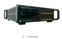

1760204989613.png

1. Large bandwidth and high precision, truly presenting signal details


The 1650E offers a maximum sampling rate of 25.6GSa/s and a maximum output instantaneous bandwidth of 10GHz, ensuring accurate generation of wideband signals. The 1650E supports 2- and 4-channel configurations and features up to 16 bits of vertical resolution, providing higher signal fidelity.

2. Ultra-fast edge and low jitter, pulse signal "as you wish"

Thanks to its high sampling rate of 25.6GSa/s, the 1650E outputs pulses with rise times as low as 46ps and a maximum amplitude of 1Vpp in single-ended DC-coupled output, meeting the requirements of most pulse testing scenarios in the automotive industry, integrated circuits, and other industries. Furthermore, the 1650E utilizes patented pulse jitter suppression technology to achieve extremely low jitter when outputting square waves and pulse signals, while supporting fine adjustment of pulse width and rising/falling edges, meeting the stringent demands for high-speed digital signals and high-precision pulses.

3. Deep storage arbitrary waveform generation, flexible adaptation to complex tests

The 1650E boasts a maximum memory depth of 8G samples per channel, supporting waveform playback up to 312.5ms even at the highest sampling rate of 25.6GSa/s, enabling long-duration, high-fidelity signal generation. The 1650E includes built-in digital and analog modulation capabilities such as ASK, FSK, PSK, AM, FM, PM, and PWM, allowing flexible arbitrary waveform programming to output complex vector-modulated signals, meeting the stringent requirements of wireless communications and RF testing.

4. Generate a variety of special signals and communication test signals to facilitate professional testing

The 1650E can not only accurately reproduce standard signals, but also flexibly simulate complex actual test environments and generate a variety of special signals including linear frequency modulation, noise signals, multi-pulse signals, etc., helping customers complete professional testing in multiple stages such as testing, verification, and production.

Please, Log in or Register to view URLs content!
 

tokenanalyst

Lieutenant General
Registered Member

Landau Technologies secures angel round financing​


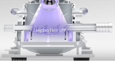
Founded in 2024, Landau Technologies specializes in the research and development, production, and technical services of specialized semiconductor manufacturing equipment. Founder Dr. Wang Hao's team, building on the research achievements of Tsinghua University's Gas Discharge Plasma Laboratory , focuses on LPP-EUV lithography light sources, a core technology in semiconductor manufacturing processes. The team is committed to providing high-power, highly stable EUV light sources to the Chinese chip manufacturing industry , achieving breakthroughs in key "bottleneck" technologies.

1760205417638.png

Landau Technologies recently completed its angel round of strategic financing, led exclusively by Zhangjiang Suiyue, an angel fund under Zhangjiang Hi-Tech Park. To date , Landau Technologies has raised over 10 million yuan.
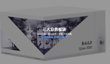
According to Zhangjiang Hi-Tech, Landau Technology currently has three core business segments:

Suiyan, which provides integrated inspection/lithography-level EUV light source systems and offers reliable EUV light source solutions to semiconductor manufacturers;
1760205509271.png
Glow - laser focusing high-power CO2 axial fast-flow laser used in EUV lithography, taking into account various industrial scenarios;
Tiansuan - focuses on the research and development and services of plasma simulation software, develops electromagnetic fluid multi-physics field simulation programs, molecular dynamics multi-scale numerical simulation programs, etc., and has been successfully embedded in industrial scenarios in the semiconductor, aerospace and other industries.​
 

tokenanalyst

Lieutenant General
Registered Member

Maike Technology received RMB100 million in Series A financing for TGV process R&D and production​


According to the Chengdu Hi-Tech Zone Science and Technology Innovation Bureau, Chengdu Maike Technology Co., Ltd. (Maike Technology) recently secured hundreds of millions of yuan in Series A funding . The funds will be used to expand TGV process R&D and production. Investors in this round include Oriza Puhua, Hidden Hills Capital (GLP), Chengdu Jiaozi Financial Holdings, Chengdu Hi-Tech Investment Ventures, and Lishi Ventures.

Maike Technology, a research achievement transfer enterprise of the University of Electronic Science and Technology of China, is also a National High-Tech Enterprise, a Sichuan Province "Specialized, Advanced, and Innovative" Small and Medium Enterprise, and the lead unit of a National Key R&D Program project. Led by national experts, the company specializes in developing advanced packaging solutions such as glass-based 3D packaging substrates, 3D microstructured glass, and chiplet 3D integration. These solutions support next-generation artificial intelligence, display, communications, the Internet of Things, and consumer electronics applications, driving the leapfrog development of integrated circuit packaging technology.

In the technology field, Maike Technology was one of the first companies internationally to develop TGV ( Through Glass Via ) technology. They proposed the TGV 3.0 concept and pioneered breakthroughs in sub-10-micron vias and vertical interconnects. The company has received numerous honors, including the National Innovation Medal and the Sichuan Provincial Technological Invention Award, establishing itself as a pioneer and leader in through-glass via technology.

According to reports, Maike Technology has built a TGV 3D packaging platform with distinct characteristics and advantages in China. It has established a production base in Songshan Lake, Dongguan, called Triassic (Guangdong) Technology Co., Ltd., which has become an internationally recognized advanced TGV process line with distinct characteristics and advantages. Furthermore, a glass wafer 3D packaging R&D base, Triassic (Sichuan) Technology Co., Ltd., has been established in Chengdu, becoming the only company in the world with both wafer-level and panel-level TGV production capabilities.​
 

jli88

Junior Member
Registered Member

Reminder that all your AI chips depend on this one ultra pure refinery in Wuxi. And I would imagine this applies to other chips.

May I ask a few questions regarding this topic?

  1. How much dysprosium is really needed in Nvidia Chips? Can they do with recycling the material from the dysprosium already exported in other products?
  2. How are the export controls going to work in practise? I assume Nvidia or even ASML are not purchasing dysprosium directly from China but it is present in some supplier or even a supplier of supplier somewhere. You would need an extremely detailed look at the supply chain and then start imposing export controls.
  3. How to tackle smuggling? China was able to export a pretty decent amount of high end chips that were export controlled. Dysprosium is needed in even smaller quantities, how do they avoid that. Already gallium controls had seepage.
 

tphuang

General
Staff member
Super Moderator
VIP Professional
Registered Member
May I ask a few questions regarding this topic?

  1. How much dysprosium is really needed in Nvidia Chips? Can they do with recycling the material from the dysprosium already exported in other products?
  2. How are the export controls going to work in practise? I assume Nvidia or even ASML are not purchasing dysprosium directly from China but it is present in some supplier or even a supplier of supplier somewhere. You would need an extremely detailed look at the supply chain and then start imposing export controls.
  3. How to tackle smuggling? China was able to export a pretty decent amount of high end chips that were export controlled. Dysprosium is needed in even smaller quantities, how do they avoid that. Already gallium controls had seepage.
they are also blocking recycling tech for dysprosium. They can certainly shut down dysprosium export if they want to. They've been doing these export licenses for several months now, so should have a good sense of who the end users are.
 
Top