Chinese semiconductor thread II

tokenanalyst

Brigadier
Registered Member
More lithography​

Ruilian New Materials: The company reserves a variety of photoresist material products, and some photoresist monomer materials have been mass-produced​


Ruilian New Materials stated on its interactive platform that photoresist materials generally have longer customer validation cycles due to their more stringent requirements for metal ion content, impurity control, and water content. The company currently has a wide range of photoresist material products in stock, with some monomeric photoresist materials already in mass production and others in the customer validation phase.
It further stated that the company's semiconductor photoresist monomers are all customized products, some of which have already been mass-produced, while others are currently undergoing customer verification. Compared with display material products, the research and development and customer verification (pilot and mass production verification) of photoresist-related products are longer. Although the company's photoresist-related product revenue is relatively small at present, the company has a large number of products in reserve. As the number of verified products increases and gradually increases in volume, they will make a significant contribution to the company's overall revenue in the future.
Notably, Ruilian New Materials initiated its strategic plan as early as August 2023, planning to invest 491 million yuan in a photoresist and high-end new materials industrialization project. Implemented by its wholly-owned subsidiary, Dali Haitai, the project aims to meet the specialized production needs of hazardous chemicals and specialty products, further expanding the company's product lines and offerings.

Please, Log in or Register to view URLs content!
 

tokenanalyst

Brigadier
Registered Member

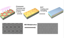
Up to 48× Density Multiplication Achieved by Directed Self-Assembly on Plasma-Trimmed Honeycomb Templates​


Achieving pattern density multiplication through direct self-assembly (DSA) is a viable path to increasing manufacturing throughput and reducing costs in photolithographic manufacturing. However, as the density multiplication factor increases, current process flows face challenges in achieving defect-free ordered arrangements with the experimentally realized multiplication factors being limited. This study proposes an innovative method to guide cylindrical PS-b-PMMA, achieving a maximum multiplication factor of 48×. The honeycomb guiding templates for DSA were fabricated through a two-step process involving lithography and trimming, resulting in long-range ordered block copolymers microdomains. The ingenious trimming of the exposure pattern doubles the density of the guiding pattern, and the resulting boomerang-shaped, triaxially symmetric template provides a more robust anchoring mechanism, demonstrating the potential for achieving high multiplication factors. Additionally, the DSA effects were validated through simulation using a coarse-grained model. This guiding scheme achieves ordered nanopore arrays with excellent placement accuracy, pattern uniformity, and transferability, offering a feasible pathway for the high-density multiplication of cylindrical phases. It presents a promising solution for scalable nanomanufacturing.

1754430203465.png

Please, Log in or Register to view URLs content!
 

gotodistance

New Member
Registered Member
What is means?


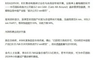
The IEEE Integrated Circuit Symposium opened at 9:00 AM on August 6th in Putrajaya, Malaysia. The most eye-catching event on the agenda was SMIC's public debut of a 2nm GAA (Gate-All-Around) transistor prototype wafer. Foreign media described this as the first public disclosure of 2nm details by a Chinese industry chain.

On-site data shows that the prototype uses a domestic substrate and multi-layer nanosheet stack, with a channel width of only 6nm. Compared with 3 nm FinFET, the equivalent performance is improved by 18% and the power consumption is reduced by 34%.

The suspense of lithography machines is also rising

Just before the meeting, ASML urgently responded to market rumors, confirming that "it has obtained permission from the Dutch government to export 0.55 NA EUV lithography machines to specific Chinese customers for 2nm research and development", but did not disclose the quantity and delivery time.

Industry insiders estimate that a single 0.55 NA device is worth approximately US$350 million. If it arrives this year, it will lay the hardware foundation for SMIC's small-batch trial production in 2026.

GxqAnTxawAEtVgD.jpg
 
Last edited:

ansy1968

Brigadier
Registered Member
Just before the meeting, ASML urgently responded to market rumors, confirming that "it has obtained permission from the Dutch government to export 0.55 NA EUV lithography machines to specific Chinese customers for 2nm research and development", but did not disclose the quantity and delivery time.

Industry insiders estimate that a single 0.55 NA device is worth approximately US$350 million. If it arrives this year, it will lay the hardware foundation for SMIC's small-batch trial production in 2026.

View attachment 157518
Impossible!!!! ASML HIGH NA laser are sourced from CYMER an American company. When SMIC order an EUVL from ASML in 2019 it was block by the American and even sabotaged it, if we were to believed this rumor and ASML is willing to sell their top of the line EUVL it only means that a commercially viable Chinese EUVL is ready for mass deployment.
 

Wahid145

Junior Member
Registered Member
What is means?


The IEEE Integrated Circuit Symposium opened at 9:00 AM on August 6th in Putrajaya, Malaysia. The most eye-catching event on the agenda was SMIC's public debut of a 2nm GAA (Gate-All-Around) transistor prototype wafer. Foreign media described this as the first public disclosure of 2nm details by a Chinese industry chain.

On-site data shows that the prototype uses a domestic substrate and multi-layer nanosheet stack, with a channel width of only 6nm. Compared with 3 nm FinFET, the equivalent performance is improved by 18% and the power consumption is reduced by 34%.

The suspense of lithography machines is also rising

Just before the meeting, ASML urgently responded to market rumors, confirming that "it has obtained permission from the Dutch government to export 0.55 NA EUV lithography machines to specific Chinese customers for 2nm research and development", but did not disclose the quantity and delivery time.

Industry insiders estimate that a single 0.55 NA device is worth approximately US$350 million. If it arrives this year, it will lay the hardware foundation for SMIC's small-batch trial production in 2026.

View attachment 157518
Anyone has more info on this? I remember few months ago there were rumor about Chinese attempt at 2nm with Huawei in Charge along with SMIC.
 

tokenanalyst

Brigadier
Registered Member

Shengmei Shanghai achieved revenue of 3.265 billion yuan in the first half of the year, with net profit increasing by 56.99% year-on-year​


On August 6, Shengmei Shanghai released its performance report for the first half of 2025, stating that its operating income in the first half of the year was 3.265 billion yuan, a year-on-year increase of 35.83%. The main reason was the strong demand in the Chinese mainland market. Relying on its technological differentiation advantages, the company successfully seized market opportunities and accumulated sufficient order reserves; the company's sales delivery and commissioning acceptance work was efficiently promoted during this period, effectively ensuring the steady growth of operating performance; the company has deeply promoted product platformization, and the product technology level and performance have continued to improve. The product series has become increasingly complete, meeting the diverse needs of customers, and market recognition has continued to increase, providing strong support for revenue growth.

Total profit was RMB 820 million, a year-on-year increase of 75.27%; net profit attributable to the parent company was RMB 696 million, a year-on-year increase of 56.99%; and net profit excluding non-recurring items was RMB 674 million, a year-on-year increase of 55.17%. This was mainly due to the growth of the company's core business income and the reduction of share-based compensation expenses.

As of the end of the first half of the year, Shengmei Shanghai's total assets were 13.289 billion yuan, a year-on-year increase of 9.56%; the net assets attributable to shareholders of listed companies were 8.24 billion yuan, a year-on-year increase of 7.49%.

The net cash flow generated from operating activities in the first half of the year was -132 million yuan, a year-on-year decrease of 129.54%, mainly due to the expansion of business scale, which led to an increase in employee salaries paid by the company, the increase in total profits, which led to an increase in the company's corporate income tax payments in this period, and a slowdown in the collection of accounts receivable.

Basic earnings per share were RMB 1.58, up 54.90% year-on-year; diluted earnings per share were RMB 1.57, up 57.00% year-on-year; and basic earnings per share after deducting non-recurring gains and losses were RMB 1.53, up 53.00% year-on-year. This was primarily due to the growth in the company's core business revenue and the reduction in share-based compensation expenses.

In the first half of the year, ACM Shanghai's core product lines achieved outstanding market performance and significant technological innovation. In the semiconductor cleaning equipment sector, according to Gartner, the company holds an 8% global market share (ranking fourth globally). According to statistics from some Chinese manufacturers, the company's single-wafer cleaning equipment market share in China exceeds 30%, ranking second among all cleaning equipment suppliers domestically and internationally. In March 2025, the company's independently developed single-wafer high-temperature SPM equipment successfully passed key customer validation, demonstrating its significant value in the manufacture of next-generation semiconductor devices. In the semiconductor electroplating equipment sector, the company holds an 8.2% global market share (ranking third globally). During the reporting period, the company delivered its 1,500th electroplating chamber for its ECP equipment, achieving full coverage of electroplating technology (front-end copper interconnect, back-end wafer-level packaging, 3D stacking, and compound semiconductors).

Please, Log in or Register to view URLs content!
 
Top