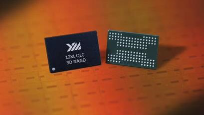
Great progress had been achieved from the flash memory front.
from cnTechPost
Yangtze Memory's 128-layer QLC flash memory debuts with highest I/O speed
2020-08-14 23:48:14 GMT+8 | cnTechPost
0
After announcing the successful development of 128-layer QLC 3D flash memory on April 13 this year, Yangtze Memory Technologies, China's top memory chipmaker under the umbrella of Tsinghua Unigroup, publicly demonstrated its 128-layer QLC 3D NAND flash memory chip at the China Electronic Information Expo held today.
Yangtze Memory showcased a 64-layer, a 128-layer stack of flash memory this time, of which the former is the first 64-layer flash memory developed and mass-produced by a Chinese company. It is based on the Xtacking stacking architecture, and the storage density per unit area is the largest in its class.
At present, the main product of Yangtze Memory's mass production is 64-layer TLC flash memory, which has been adopted by a large number of manufacturers' SSD hard drives.
The 128-layer QLC flash memory shown by Yangtze Memory is the next generation product after 64-layer flash memory, based on the Xtacking 2.0 architecture.
According to the company, the uniqueness of this product is that it is the industry's first 128-layer QLC 3D NAND. It has the highest storage density per unit area, the highest I/O transmission speed and the highest single NAND flash memory chip capacity among known models.
In terms of performance, Yangtze Memory revealed that the two products have 1.6Gbps I/O read and write performance, and the single 3D QLC capacity is as high as 1.33Tb, which is 5.33 times that of the previous generation of 64 layers.

