You are using an out of date browser. It may not display this or other websites correctly.
You should upgrade or use an alternative browser.
You should upgrade or use an alternative browser.
News on China's scientific and technological development.
- Thread starter Quickie
- Start date
A beautiful conversation about chip between FairAndUnbiased ,antonius123 , and our own Figaro cross post from PAKISTAN DEFENSE FORUM
From FairAndUnbiased
From FairAndUnbiased
For an article purporting to talk about what Ren Zhengfei is thinking, there is not a single quote from Ren Zhengfei himself on here.
Whoever wrote this article shows a profound lack of understanding of what semiconductors are used for and what parts of the business are profitable.
Huawei makes little from its smartphone business AND its smartphone business is the one primarily impacted by the TSMC restrictions. Its 5G business is both more profitable and less impacted by TSMC restrictions.
7 nm is not cheaper than 65+ nm. It is much cheaper to implement a 65 nm process because even though you need more chips and power for equivalent performance, each chip requires less processing steps and/or less expensive equipment.
For 65 nm chips for instance you can get away with single patterning dry DUV lithography, but for 7 nm you either need EUV lithography (10x higher price per machine, lower yield, need to completely change process chemistry) or immersion DUV lithography with double patterning (half the yield, much higher defect rates, double or more price per machine). 65 nm chips can use cheaper processes like silicon dioxide gate dielectric with polysilicon gate (very cheap, requires only silicon and oxygen), but lower processes requires exotic materials like hi-K dielectrics and tungsten gates (which must be deposited by highly specialized ALD/CVD processes).
The advantage of 7 nm comes from lower power consumption and higher computational speed - good for mobile processor applications (phones/tablets/laptops), but 5G base stations don't need that - they're plugged into the grid. Most 5G modems are on 14-28 nm processes, some are on 40 nm processes. Only ZTE is using a 7 nm process modem right now I believe.
antonius123 said:
FairAndUnbiased said:What Huawei lack, to supply 5G equipment, at least for China market?
Design: nothing. Huawei has proprietary modem and mobile processor chip designs. It controls the full intellectual property ecosystem.
Fabrication: Balong 5000 modem is fabbed on 7 nm TSMC. It may be switched to Samsung (which has a fully non-American production line) 7 nm or SMIC 7 nm. Or, they'll tape out a 14 nm version. I don't think modems are tied to 7 nm process since power efficiency is not critical for them.
Kirin 910 mobile processor is fabbed on 7 nm TSMC, but they've already taped out Kirin 710A on 14 nm SMIC.
Figaro said:
FairAndUnbiased said:When is SMIC 7nm going to start? Also, how is China going to progress below 7nm if it does not have ASML's EUV tech?
it probably can't until China developts its own lithography system. 7 nm is about the limit for immersion lithography. but neither can the US semiconductor flagships Intel and Global Foundries. What's worse, they didn't fail for not having EUV, but because they just can't get it to work with high enough yield and with a substantial enough advantage over 10/14 nm.
Intel is now thinking of outsourcing next generation CPUs to TSMC or maybe even going full fabless, while Global Foundries used to be AMD's premier fab but now decided to shift towards automotive and RF applications because those don't require sub 14 nm. GloFo sold its EUV instrument and laid off/reassigned the EUV staff.
Right now, even Samsung is struggling with EUV, since their yields are not good and they have trouble getting customers. TSMC has basically completely dominated the foundry market.
Interesting ... so China (and everyone else besides TSMC) will be stuck on the 7nm for the foreseeable future.
Basically, for logic/foundry, TSMC is tier 1, Intel/Samsung are tier 2, GloFo/SMIC/UMC are tier 3 (with 14 nm tech).
Then you have non-14 nm fabs like Huahong, STMicro, etc. who are 2 generations behind at 28 nm. TBH, UMC and GloFo would fit in here, if they didn't license 14 nm tech from IBM and Samsung, respectively.
Below that you have trailing edge foundries like TowerJazz, Infineon and STMicro who work at 45+ nm tech.
Finally, you have automotive, IOT, optoelectronics (camera sensor, LED, display), power, etc. fabs like Analog Devices, Texas Instruments, MagnaChip, SK Hynix, Dongbu, X-Fab, Sony, Microchip, etc. who work at low level nodes like 130-350 nm.
You don't need bleeding edge for this stuff; a bunch of industrial hardware runs on 8 bit, 130 nm process Atmel/Microchip stuff from 2005.
The gap between each tier is gigantic. For example, many Analog Devices and Texas Instruments fabs are still around from the 1980's and still work on 200 mm wafers at 350 nm tech.
Multipatterning isn’t just more expensive, it’s more complicated, slower, can hurt yields, and is also more prone to introducing delays in your process. That’s why EUV for smaller nodes is a really big deal.The Changchun Institute has developed a set of Projection Lens/Optics but how this compares to the Carl Zeiss Optics in the Asml EUV machine is unknown. Hopefully the Changchun/Smee EUV has a conparable resolution to the latest EUV from Asml. If not........you can always use Multi Patterning to get there. Asml will be releasing its next generation EUV in 2022 with improved Optics, i think 0.55.
I suppose the choice of DUV or EUV is up to the client based on the cost of the machine and operational cost. The DUV Multi Patterning for 5nm would be more expensive due to more Masks being required but the EUV machine will be more expensive to acquire. But i suspect that the DUV for 5nm might come out before the EUV.
hi WTAN,
Regarding Gigaphoton, they had set up an office in Shanghai, will they sell their LPP to SMEE? or they are also bound by the same Waseenar Agreement?
Gigaphoton in 2019 developed a 250W LPP Light source. The problem for Gigaphoton is that ASML will never buy this LPP from them as Cymer USA is the sole supplier to ASML. The US unfortunately will not allow Gigaphoton to sell to China due to Waseenar Agreement. The only way for Gigaphoton to evade this is to set up a joint venture factory in China to produce this Light Source. Will this happen?
In any case China is developing its own LPP light source and when it succeeds this will be bad news for Gigaphoton.
Huawei had develop a EDA tool for 7nm
continued conversation between FairAndUnbiased and antonius123 (PAKISTAN DEFENSE FORUM)
FairAndUnbiased said:
continued conversation between FairAndUnbiased and antonius123 (PAKISTAN DEFENSE FORUM)
antonius123 said:
OK, at least Huawei still can survive with 5G equipment and lower end smartphone, except the high end smartphone that require the most advance chip.
But regarding SMIC expansion for 7nm, means they need to buy additional equipment from lithography, wafer surface conditioning, dicing, etc till electronic design automation (EDA) software, that means the expansion is fragile and could be subject to US ban?
Right now, and for the foreseeable future, there is no way around Synopsys, Cadence, or Mentor Graphics EDA software if you want to design modern chips—and all three are US companies, according to this:
Click to expand...
FairAndUnbiased said:
Lithography is the bottleneck but US doesn't have it either. Now it's pretty much ASML tier 1 (EUV), Nikon tier 2 (Immersion Ar-F, 7 nm capable), and SMEE/Canon competing at tier 3 (~90 nm ArF dry etch) with SMEE moving up to tier 2 with Nikon soon. AMAT and Lam compete in roughly the same sectors (deposition/etch), but there they also compete with AMEC and Naura in China, and TEL in Japan. They have KLA Tencor for metrology, but there's also Hitachi and Zeiss.
What do you think is going to happen if they ban US EDA from being used in China? Chinese companies are going to stop paying for US EDA software. They're not going to stop using it. The lawyers referenced won't be able to do jack shit if the companies aren't listed or have assets overseas, and most Chinese semiconductor companies are purely domestic focused with the exception of Huawei and ZTE. They don't want to play this card, they have much more to lose.
Sometimes we need to reflect and understand the hard work and hardship SMIC had gone thru to develop their 14nm and 7nm tech.
The reason Intel failed in their 7nm & 10nm endeavor from Song Hong (PAKISTAN DEFENSE FORUM)
Intel fire Renduchintala, Chief Engineering Officer, while 7nm or even 10nm keep failing. When this guy came on board, he immediately hired 2 more Indians reporting to him. They were Raja Koduri and Randhir Thakur.
Other than engineering, Intel was infested by Indians everywhere.
The only place Intel can go is Chapter 11.
TSMC 5nm is already stable for production.
![[IMG] [IMG]](https://newsroom.intel.com/wp-content/uploads/sites/11/2016/03/Murthy_Renduchintala_print_01-240x360.jpg)
Intel said Monday that Venkata “Murthy” Renduchintala, the chipmaker’s chief engineering officer and group president of its technology, systems architecture and client group, will resign on August 3.
Same case as when Singapore sign up CECA with India. The Indian executives come in with big talk and run companies into ground.
Hi hullopilllw,Same case as when Singapore sign up CECA with India. The Indian executives come in with big talk and run companies into ground.
Do you think Microsoft,Google and Nokia will also suffer the same fate, their CEO are all indian? And also I had seen a pattern of discrimination against EAST ASIAN in particular for high position job, the caucasian dont trust us or as our trait, we dont talk to much.
hi WTAN, Skywatcher and SuperDog
need your opinion on this article, and its usage
from cnTechPost
Chinese company develops new kind of lithography equipment
2020-07-28 19:22:02 GMT+8 | cnTechPost
0
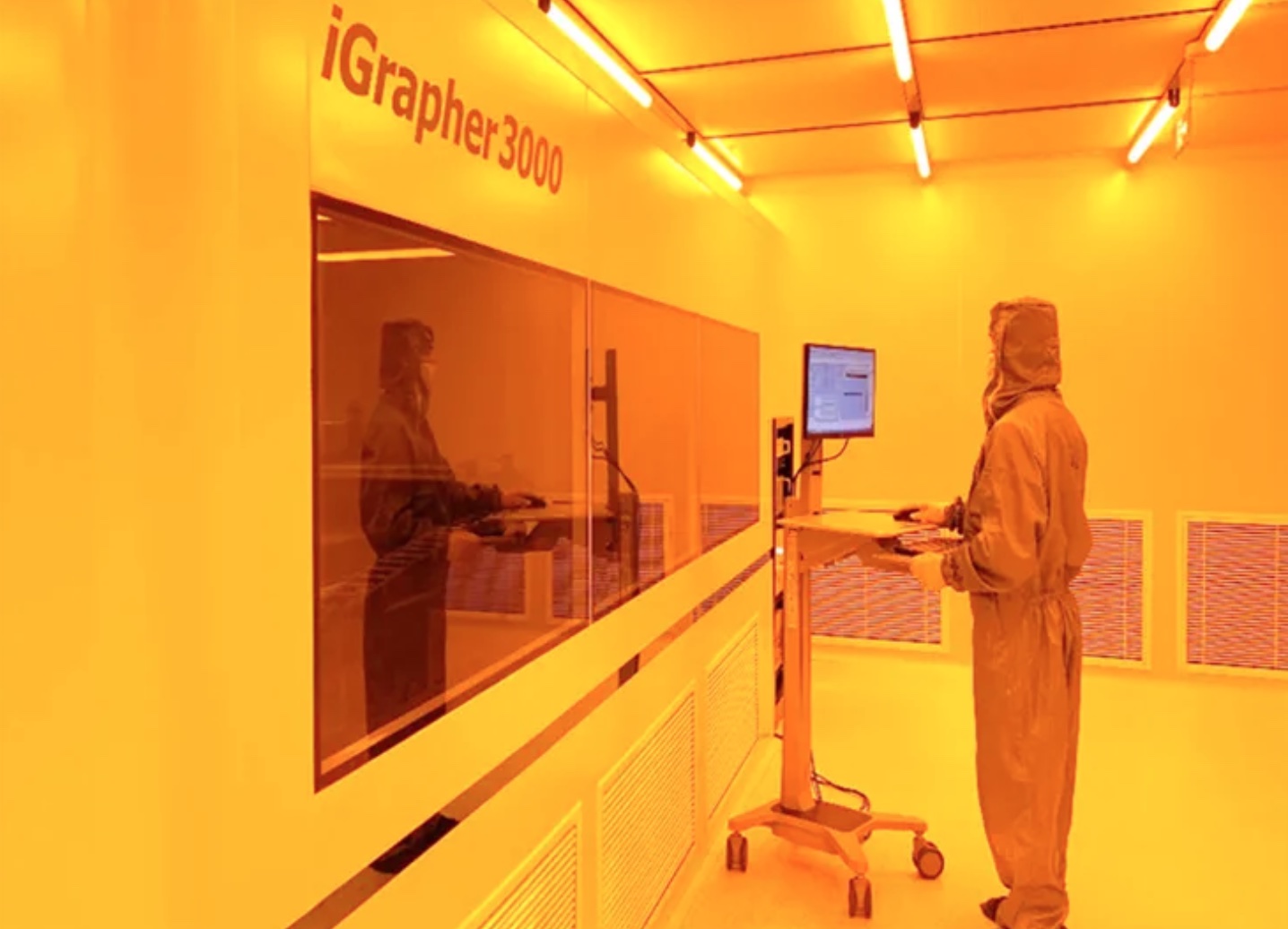
SVG Group, a Chinese technology company, that it has launched industrial production of its iGrapher 3000, the world's first large-scale UV-3D direct lithography machine.
SVG Group is engaged in the design, development, and manufacture of micro- and nano-structured products and manufacturing equipment, as well as the provision of related technical research and development services.
The iGrapher3000 is mainly used for 3D lithography of micro-nano-structured topography on large substrates.
It is a new platform for the design, development, and manufacture of novel materials and advanced optoelectronic devices, and can be called the cornerstone equipment of the optoelectronic industry.
From planar lithography of integrated circuits to 3D lithography of "micro-structured topography" of optoelectronics, iGrapher3000 provides an advanced means for the design of novel materials and functional optoelectronic devices.
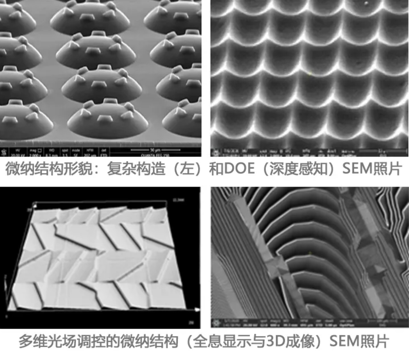
Below are photos of the iGrapher3000 UV 3D lithography rig (110" format, 2500mmx1500mm) and SEM photos of the micro-nano topography.
The iGrapher3000 has been installed in the iVTouch factory, where its first industrial application is a deep groove structured microcircuit mold of a large transparent conductive film.
It will also be used in the development and industrialization of large-area flat panel imaging, flexible conductive devices and holographic and 3D display applications.
According to SVG Group, Dr. Pu Donglin has led the research staff in the development of 3D lithography, nanolithography hardware and software, data processing algorithms, and precision control technology for more than a decade.
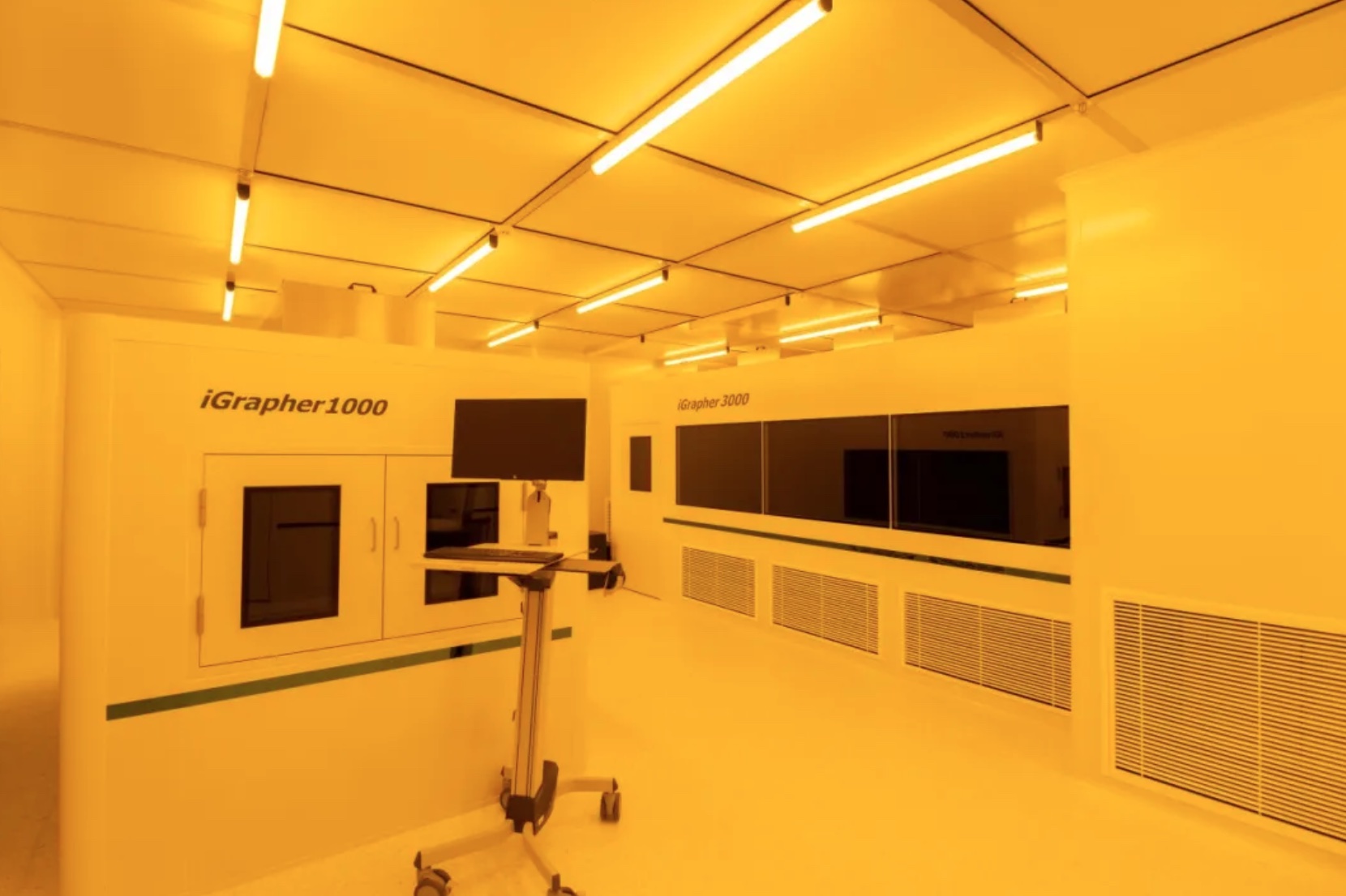
After several rounds of iterations, they have overcome major bottlenecks in 3D lithography and successfully developed a series of UV 3D direct lithography equipment, represented by the iGrapher3000, for industrial applications.
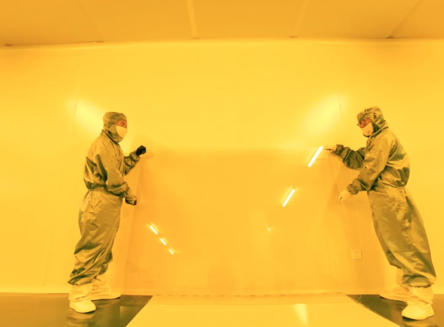
The iGrapher3000 is the first of its kind to enable continuous-plane microstructured large-area flat-panel devices on 110-inch glass substrates with depths ranging from 50nm to 20 microns.
It can be built to support 110" thick gluing process (2 microns to 25 microns) on photoresist board for subsequent industrial production of printing plates.
In the chip industry, there are two types of lithography machines: the first is projection lithography, which microscopes and lithographs photo masked graphics onto silicon wafers to prepare integrated circuit graphics.
It has a thinnest line width of 5nm, such as ASML extreme ultraviolet EUV projection lithography machine.
Japanese Nikon's i-series and Canon's FPA series of high-precision step projection lithography are also of this type.
The second type is Direct Writing Lithography, which is used for the preparation of the chip photomask at 0.25-micron node and above, and the partial photomask at 0.18-micron node and below.
The remaining node masks, prepared with electron beam lithography EBL, account for about 25%.
This includes American Applied Materials (AM) ALTA lithography.
In the display panel industry, Mycronic Sweden and Prexision 10 laser direct-write lithography system are used for 10th-generation line photomask preparation.
Nikon large projection scanning lithography (FX series) is used to scan and lithograph photomask graphics onto large size substrates to form TFT circuit graphics.
Therefore, in IC integrated circuits, display panels, etc., Direct Writing Lithography is used to prepare design data onto a photoresist substrate to become a photomask for back-channel projection lithography replication.
Both of the above two types of lithographs belong to the "flat pattern" lithographs, which are used in the thin-lithography process.
Both Direct Writing Lithography and Projection Lithography are key equipment in the integrated circuit and photonics industry. Direct Writing Lithography belongs to the source type key link, called Pattern Generator.
The iGrapher3000's "3D Topography" lithography belongs to the thick glue process.
It is mainly used for the preparation of optoelectronic materials and devices, the role is to prepare the design data onto a thick photoresist substrate, to become a three-dimensional shape of the nano printing plate, for a post-imprinting copy.
The iGrapher3000 is a powerful 3D lithography system that exposes the design data in a 3D navigational flight scan mode, creating a 3D microstructure in one scan.
It supports multi-format 2D and 3D model data files, lithography of hundreds of Tb data volume, and write speed greater than 3Gbps.
It has a fast lithography function with data processing/transfer/write synchronization.
It has an area of 110 inches, a lithography depth range of 50 nm to 20 microns, and a depth resolution of 10 nm.
Theoretically, the micro-nano structure topography has 5-dimensional controllable variables that support various optical fields and electromagnetic long modulation material and device design and fabrication.
As a comparison, for chip extreme ultraviolet projection lithography (EUV), pursuing extremely fine line widths (already up to 5 nm).
They are facing difficulties in extreme precision control and high yields (extreme ultraviolet light source, motion platform, and register accuracy), projection lithography for chips, microcopy of graphics with a photomask, and issues not involving massive data processing.
Direct write lithography (LDW) for photomask converts regular circuit graphics into photomask to form a display TFT photomask.
Unlike the thin-gel lithography process for integrated circuits, 3D lithography for the topography of micro-nano structures pursues topography and relative alignment accuracy (depending on the application).
The difficulty lies in massive data processing and transmission (hundreds of Tb), functional design of large area structures and advanced algorithms, and fidelity processes such as 3D lithography and 3D proximity compensation.
Its depth range: 50nm~20 microns, precision range: 1nm~100nm.
It can be seen that 3D lithography is significantly different from the previous 2D lithography in terms of function and use.
The iGrapher3000 opens up new channels for the research and industrial innovation of novel optoelectronic materials and functional devices.
It is mainly used for the fabrication of micro-nano topography and deep structures including large-size optoelectronic devices, super constructive surface materials, and functional optoelectronic devices.
This includes large-size transparent circuit graphics, high-precision flexible touch sensors, high-brightness projection screens, holographic 3D displays, MiniLED circuit backsplashes, high-brightness uniformity plates, virtual and real fusion photonic devices, and large-diameter transparent electromagnetic shielding materials.
The iGrapher 3000 is also used in the photomask fabrication for flat panel displays and flexible electronics and provides a strategic R&D resource for the design and fabrication of high-precision large-aperture thin-film lenses.
SVG's Lithography Equipment Division has a solid foundation in lithography technology and equipment and has developed a variety of lithography equipment such as the MiScan200 (8"~12") for MEMS chips, the MicroLab (4"~8") for MEMS chips, and the MicroLab (4"~8") for MEMS chips. ") and NanoCrystal (8"~32"), a nano-lithography device for super-surface, naked-eye 3D display, and optoelectronic device research.
need your opinion on this article, and its usage
from cnTechPost
Chinese company develops new kind of lithography equipment
2020-07-28 19:22:02 GMT+8 | cnTechPost
0

SVG Group, a Chinese technology company, that it has launched industrial production of its iGrapher 3000, the world's first large-scale UV-3D direct lithography machine.
SVG Group is engaged in the design, development, and manufacture of micro- and nano-structured products and manufacturing equipment, as well as the provision of related technical research and development services.
The iGrapher3000 is mainly used for 3D lithography of micro-nano-structured topography on large substrates.
It is a new platform for the design, development, and manufacture of novel materials and advanced optoelectronic devices, and can be called the cornerstone equipment of the optoelectronic industry.
From planar lithography of integrated circuits to 3D lithography of "micro-structured topography" of optoelectronics, iGrapher3000 provides an advanced means for the design of novel materials and functional optoelectronic devices.
Below are photos of the iGrapher3000 UV 3D lithography rig (110" format, 2500mmx1500mm) and SEM photos of the micro-nano topography.

The iGrapher3000 has been installed in the iVTouch factory, where its first industrial application is a deep groove structured microcircuit mold of a large transparent conductive film.
It will also be used in the development and industrialization of large-area flat panel imaging, flexible conductive devices and holographic and 3D display applications.
According to SVG Group, Dr. Pu Donglin has led the research staff in the development of 3D lithography, nanolithography hardware and software, data processing algorithms, and precision control technology for more than a decade.

After several rounds of iterations, they have overcome major bottlenecks in 3D lithography and successfully developed a series of UV 3D direct lithography equipment, represented by the iGrapher3000, for industrial applications.
The iGrapher3000 is the first of its kind to enable continuous-plane microstructured large-area flat-panel devices on 110-inch glass substrates with depths ranging from 50nm to 20 microns.
It can be built to support 110" thick gluing process (2 microns to 25 microns) on photoresist board for subsequent industrial production of printing plates.

In the chip industry, there are two types of lithography machines: the first is projection lithography, which microscopes and lithographs photo masked graphics onto silicon wafers to prepare integrated circuit graphics.
It has a thinnest line width of 5nm, such as ASML extreme ultraviolet EUV projection lithography machine.
Japanese Nikon's i-series and Canon's FPA series of high-precision step projection lithography are also of this type.
The second type is Direct Writing Lithography, which is used for the preparation of the chip photomask at 0.25-micron node and above, and the partial photomask at 0.18-micron node and below.
The remaining node masks, prepared with electron beam lithography EBL, account for about 25%.
This includes American Applied Materials (AM) ALTA lithography.
In the display panel industry, Mycronic Sweden and Prexision 10 laser direct-write lithography system are used for 10th-generation line photomask preparation.
Nikon large projection scanning lithography (FX series) is used to scan and lithograph photomask graphics onto large size substrates to form TFT circuit graphics.
Therefore, in IC integrated circuits, display panels, etc., Direct Writing Lithography is used to prepare design data onto a photoresist substrate to become a photomask for back-channel projection lithography replication.
Both of the above two types of lithographs belong to the "flat pattern" lithographs, which are used in the thin-lithography process.
Both Direct Writing Lithography and Projection Lithography are key equipment in the integrated circuit and photonics industry. Direct Writing Lithography belongs to the source type key link, called Pattern Generator.
The iGrapher3000's "3D Topography" lithography belongs to the thick glue process.
It is mainly used for the preparation of optoelectronic materials and devices, the role is to prepare the design data onto a thick photoresist substrate, to become a three-dimensional shape of the nano printing plate, for a post-imprinting copy.
The iGrapher3000 is a powerful 3D lithography system that exposes the design data in a 3D navigational flight scan mode, creating a 3D microstructure in one scan.
It supports multi-format 2D and 3D model data files, lithography of hundreds of Tb data volume, and write speed greater than 3Gbps.
It has a fast lithography function with data processing/transfer/write synchronization.
It has an area of 110 inches, a lithography depth range of 50 nm to 20 microns, and a depth resolution of 10 nm.
Theoretically, the micro-nano structure topography has 5-dimensional controllable variables that support various optical fields and electromagnetic long modulation material and device design and fabrication.
As a comparison, for chip extreme ultraviolet projection lithography (EUV), pursuing extremely fine line widths (already up to 5 nm).
They are facing difficulties in extreme precision control and high yields (extreme ultraviolet light source, motion platform, and register accuracy), projection lithography for chips, microcopy of graphics with a photomask, and issues not involving massive data processing.
Direct write lithography (LDW) for photomask converts regular circuit graphics into photomask to form a display TFT photomask.
Unlike the thin-gel lithography process for integrated circuits, 3D lithography for the topography of micro-nano structures pursues topography and relative alignment accuracy (depending on the application).
The difficulty lies in massive data processing and transmission (hundreds of Tb), functional design of large area structures and advanced algorithms, and fidelity processes such as 3D lithography and 3D proximity compensation.
Its depth range: 50nm~20 microns, precision range: 1nm~100nm.
It can be seen that 3D lithography is significantly different from the previous 2D lithography in terms of function and use.
The iGrapher3000 opens up new channels for the research and industrial innovation of novel optoelectronic materials and functional devices.
It is mainly used for the fabrication of micro-nano topography and deep structures including large-size optoelectronic devices, super constructive surface materials, and functional optoelectronic devices.
This includes large-size transparent circuit graphics, high-precision flexible touch sensors, high-brightness projection screens, holographic 3D displays, MiniLED circuit backsplashes, high-brightness uniformity plates, virtual and real fusion photonic devices, and large-diameter transparent electromagnetic shielding materials.
The iGrapher 3000 is also used in the photomask fabrication for flat panel displays and flexible electronics and provides a strategic R&D resource for the design and fabrication of high-precision large-aperture thin-film lenses.
SVG's Lithography Equipment Division has a solid foundation in lithography technology and equipment and has developed a variety of lithography equipment such as the MiScan200 (8"~12") for MEMS chips, the MicroLab (4"~8") for MEMS chips, and the MicroLab (4"~8") for MEMS chips. ") and NanoCrystal (8"~32"), a nano-lithography device for super-surface, naked-eye 3D display, and optoelectronic device research.
Skywatcher
Captain
It's for making flat panel displays, I believe.
