You are using an out of date browser. It may not display this or other websites correctly.
You should upgrade or use an alternative browser.
You should upgrade or use an alternative browser.
News on China's scientific and technological development.
- Thread starter Quickie
- Start date
The world's first architecture moves towards AGI! Tsinghua University team releases smart optical chip "Tai Chi"!
With the emergence of various large models and deep neural networks, how to create next-generation AI chips that meet the development of artificial intelligence and have both large computing power and high energy efficiency has become a hot topic at the international forefront. The research group of Associate Professor Fang Lu from the Department of Electronic Engineering of Tsinghua University and the research group of Academician Dai Qionghai from the Department of Automation abandoned the traditional electronic deep computing paradigm and took a new approach, creating the first distributed breadth intelligent optical computing architecture to develop the world's first large-scale interference diffraction heterogeneous integrated chip "Tai Chi" ( Taichi), achieving 160TOPS/W general intelligent computing. The research results were published in the latest issue of "Science" on April 12, Beijing time.

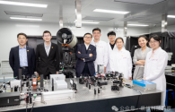
This is a table top optical setup. They need to shrink this down into a chip.The world's first architecture moves towards AGI! Tsinghua University team releases smart optical chip "Tai Chi"!
With the emergence of various large models and deep neural networks, how to create next-generation AI chips that meet the development of artificial intelligence and have both large computing power and high energy efficiency has become a hot topic at the international forefront. The research group of Associate Professor Fang Lu from the Department of Electronic Engineering of Tsinghua University and the research group of Academician Dai Qionghai from the Department of Automation abandoned the traditional electronic deep computing paradigm and took a new approach, creating the first distributed breadth intelligent optical computing architecture to develop the world's first large-scale interference diffraction heterogeneous integrated chip "Tai Chi" ( Taichi), achieving 160TOPS/W general intelligent computing. The research results were published in the latest issue of "Science" on April 12, Beijing time.
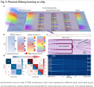
View attachment 128186
Photonics.This is a table top optical setup. They need to shrink this down into a chip.

Photonic neuromorphic architecture for tens-of-task lifelong learning
Abstract
Scalable, high-capacity, and low-power computing architecture is the primary assurance for increasingly manifold and large-scale machine learning tasks. Traditional electronic artificial agents by conventional power-hungry processors have faced the issues of energy and scaling walls, hindering them from the sustainable performance improvement and iterative multi-task learning. Referring to another modality of light, photonic computing has been progressively applied in high-efficient neuromorphic systems. Here, we innovate a reconfigurable lifelong-learning optical neural network (L2ONN), for highly-integrated tens-of-task machine intelligence with elaborated algorithm-hardware co-design. Benefiting from the inherent sparsity and parallelism in massive photonic connections, L2ONN learns each single task by adaptively activating sparse photonic neuron connections in the coherent light field, while incrementally acquiring expertise on various tasks by gradually enlarging the activation. The multi-task optical features are parallelly processed by multi-spectrum representations allocated with different wavelengths. Extensive evaluations on free-space and on-chip architectures confirm that for the first time, L2ONN avoided the catastrophic forgetting issue of photonic computing, owning versatile skills on challenging tens-of-tasks (vision classification, voice recognition, medical diagnosis, etc.) with a single model. Particularly, L2ONN achieves more than an order of magnitude higher efficiency than the representative electronic artificial neural networks, and 14× larger capacity than existing optical neural networks while maintaining competitive performance on each individual task. The proposed photonic neuromorphic architecture points out a new form of lifelong learning scheme, permitting terminal/edge AI systems with light-speed efficiency and unprecedented scalability.
Academician Zhu Shining’s team: Thin film lithium niobate photonic chip production line officially launched
On April 11, the launch ceremony of the lithium niobate photonic chip production line of Jiangsu Nanjing Nanzhi Advanced Optoelectronics Integration Technology Research Institute (hereinafter referred to as "Nanzhi Optoelectronics") was held in Nanjing Jiangbei New District .
The project is equipped with 350 million yuan worth of equipment and a 5,000m2 ultra -clean room, covering the core processes of the entire industry chain, with a monthly production capacity of 1,000 wafers. The production line launched this time has a series of core technology processes such as photolithography, etching, coating, grinding and polishing, and wet methods, which means that the industrialization of domestic thin film lithium niobate photonic chips has made important progress.
It is understood that in 2018, with the support of Nanjing University and Nanjing Jiangbei New District, Zhu Shining, currently an academician of the Chinese Academy of Sciences and director of the Jiangsu Provincial Optoelectronic Technology Innovation Center, led a team to implement Nanzhi Optoelectronics in the Industrial Technology Research and Innovation Park of the New District and was responsible for the construction and operation of optoelectronic public technologies. Platform, aiming at the needs of next-generation optoelectronic chip technology in basic materials, device processes, etc., to carry out research and development work.
At the beginning of this year, Nanzhi Optoelectronics started the construction of the second phase of the platform. Currently, the second phase of the platform has certain mass production capabilities. A batch of 8-inch biological genetic detection chips just rolled off the production line a month ago. All relevant performance indicators meet customer customization requirements. Zhu Shining said that in the future, based on the lithium niobate photonic chip production line, Nanzhi Optoelectronics will be able to provide chip research and development and tape-out support to domestic and foreign optoelectronic companies.
Chinese scientists increase F-22 fighter jet’s radar signature 60,000 times with new detection method: study
- Researcher Xie Junwei and team say innovation enables China’s radar system to pinpoint F-22 real-time position with remarkable accuracy
- Impact of study on US military’s F-22 fighter jet could be great given range of its air-to-air missiles and required radius for ground bomb attacks: team
manqiangrexue
Brigadier
This... should not have been published. I do not understand why this would be declassified.Chinese scientists increase F-22 fighter jet’s radar signature 60,000 times with new detection method: study
- Researcher Xie Junwei and team say innovation enables China’s radar system to pinpoint F-22 real-time position with remarkable accuracy
- Impact of study on US military’s F-22 fighter jet could be great given range of its air-to-air missiles and required radius for ground bomb attacks: team
It's scmp though.This... should not have been published. I do not understand why this would be declassified.
Although sometimes they some times talk about papers that might have some influence or use in the future (most of the time, the paper is just a paper with low to no impact).
manqiangrexue
Brigadier
This should have been sealed in a file stamped "TOP SECRET" in a vault in ZhongNanHai... if it were true.It's scmp though.
Although sometimes they some times talk about papers that might have some influence or use in the future (most of the time, the paper is just a paper with low to no impact).
