TECHNOLOGY DEVELOPMENT
EPI-Wafer Growth Technology
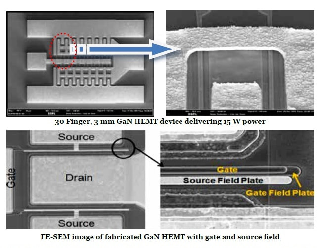
AlGaN/GaN hetero-structures having a two dimensional (2D) electron gas with a high electron density of ~1013 cm-2 and electron mobility of ~2000 cm-2 V-1s-1 are required for fabrication of high performance HEMT devices. A typical GaN HEMT hetero-structures consists of a multilayer hetero-epitaxial structure with strict control over composition as well as thicknesses at nanometer scale. The desired smoothness/abruptness of various interfaces at sub-nanometer level requires atomic scale control over growth process. Metal Organic Chemical Vapour Deposition (MDCVD) was selected for developing AlGaN/GaN HEMT epi-wafer growth process for its capability of scaling up for volume production and low manufacturing cost. A specially designed MOCVD reactor was established and a production worthy GaN HEMT epi-wafer growth technology was developed with sustained R&D efforts. A variety of crystalline substrate options, namely, Sapphire, SiC and Si, were explored for growing the desired epitaxial hetero-structures. However, the technology development was finally confined on SiC due to its least mismatch in lattice constant and thermal expansion coefficient with GaN. Further, a high thermal conductivity of SiC renders it most suitable for high power RF applications. The main challenges in developing the GaN HEMT material technology included achieving the desired 2D electron density and mobility with reduced dislocation density and control over impurities acting as deep electron traps. Other crucial requirements for AlGaN/GaN HEMT structure included (a) the growth of high resistivity GaN buffer layer, (b) precisely controlled 1 nm AlN exclusion layer with sharp interfaces and (c) growth of crack free AlGaN layers with step flow morphology while maintaining minimum particulate generation during growth. The indigenous GaN HEMT materials technology is matured and device quality epi-wafers are regularly produced for fabrication of Power HEMT devices and MMICs.
...............

