Germany Carl Zeiss, heart of Dutch ASML Lithography Equipment.

Status
Not open for further replies.

Biscuits

Colonel
Registered Member
Semiconductor industry is very much important to the strategic defence of China. Extremely important. As far as I know, the F35 core processors are from Harris and seems to be Intel designs. China needs a strong semiconductor industry for better, strong and reliable C4ISTAR capabilities too.

The core processors for PLA hardware seems to be from state owned institutes. AFAIK they have no relation with civilian companies like HiSilicon, TSMC or Tsinghua.

Even if they had wanted to, they could not acquire equipment like the one detailed in this thread? The law prohibit any foreign person/organization/equipment from working on and/or providing items related to national security. Unless there is a talk of an official sale where the govt has approved purchase of these specific machines to the defense industry, it is not really relevant to strategic defense.
 

tidalwave

Senior Member
Registered Member
There’s a lot of technical discussion that can be undertaken, I just feel like a thread on Dutch stuff should be in the world forum, unless it is co produced with China(?)
.

I think you got it wrong. This has direct relationship with China. Strategic defense doesn't mean only arms/weapons but economic, political, and technology security aspect as well. ASML is only one capable of EUV 7nm or below. No other vendor provides that.
If US-China trade talk break down and no deal, next step for US would be tighter export control. Because ASML uses some US component so it will implicate ASML export to China which will directly affect China semiconductor industry and hence its overall national security as well. You have to look at the big picture.
 

tidalwave

Senior Member
Registered Member
Relationship between Field facet mirror and pupil facet mirror of illuminator . The illuminator light then focus to the mask/reticle or AKA "chip design"
The illuminator uses mirrors while projection optics use lens.
upload_2019-4-30_2-21-44.png


NA stands for Numerical Aperture. Bigger NA needs bigger mirrors. and lens. Bigger NA means better optical resolution.

upload_2019-4-30_2-24-55.png

upload_2019-4-30_2-26-48.png
upload_2019-4-30_2-28-55.png
 

Xizor

Captain
Registered Member
Relationship between Field facet mirror and pupil facet mirror of illuminator . The illuminator light then focus to the mask/reticle or AKA "chip design"
The illuminator uses mirrors while projection optics use lens.
View attachment 52120


NA stands for Numerical Aperture. Bigger NA needs bigger mirrors. and lens. Bigger NA means better optical resolution.

View attachment 52121

View attachment 52122
View attachment 52123
I don't know if China has any Carl Zeiss equivalent. Who are the best lens makers in China? Are they state owned ? Any new startups ?
 

tidalwave

Senior Member
Registered Member
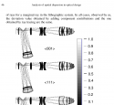
A PHD thesis on optical design for Deep DUV lithograph system. It uses Zemax simulation software for optical system.
Lens are made from crystal, the orientation of of crystal is important, 001, 010, 011

Please, Log in or Register to view URLs content!


The Zemax software can be downloaded from here. I use the software, its pretty robust able to simulate all kinds of optical configuration based on individual len material, size and distance and get the final resolution. Download it and unzipped it and read the instruction how to use it.

Please, Log in or Register to view URLs content!


Below is pic from the PHD thesis on Deep DUV lithograph systemupload_2019-5-19_22-49-57.pngA
 

antiterror13

Brigadier
SMIC: 14nm FinFET in Risk Production; China's First FinFET Line To Contribute Revenue by Late 2019
Please, Log in or Register to view URLs content!


SMIC, the largest contract maker of semiconductors in China, announced this month that it would start commercial production of chips using its 14 nm FinFET manufacturing technology by the end of the year. This is the first FinFET manufacturing line in China, making it a notable development for a country that already houses a significant number of fabs, as the world's leading-edge manufacturers never installed FinFET technology in China for geopolitical and IP reasons. SMIC in turn seems to expect a rather rapid ramp of its 14 nm node, as it anticipates the new manufacturing line will meaningfully contribute to its revenue before the end of the year.

According to SMIC, their 14 nm FinFET manufacturing technology was developed entirely in-house and is expected to significantly increase transistor density, increase performance, and lower power consumption of chips when compared to devices made using the company’s 28 nm process that relies on planar transistors. Earlier this year it was expected that SMIC would start production of 14 nm chips already in the first half of 2019, so the firm seems to be a little behind the schedule. Nonetheless, an in-house FinFET process technology is quite a breakthrough for a relatively small company that puts it into a club with just five other foundries with FinFET technologies.

One interesting thing that SMIC said about its 14 nm FinFET volume ramp is that it expects the process to have a significant revenue contribution already by the end of the year. Meanwhile, keeping in mind that right now SMIC only has two relatively small 300-mm HVM fabs (which are currently used for 28 nm – 65 nm nodes) that are heavily utilized generating 40 ~ 49% of the company’s revenue (
Please, Log in or Register to view URLs content!
), it is difficult to imagine SMIC making loads of 14 nm chips in 2019.

Overview of SMIC's Fabs
Process Technologies Capacity
Wafer Starts per Month Location
BJ 200mm 90 nm - 150 nm 50,000 Beijing, China
300mm 28 nm - 65 nm 35,000
SH 200 mm 90 nm - 350 nm 120,000 Shanghai ,China
300 mm 28 nm - 65 nm 20,000
SZ 200 mm 90 nm - 350 nm 60,000 Shenzhen, China
300 mm 28 nm - 65 m 3,000
TJ 200 mm 90 nm - 350 nm 50,000 Tianjin, China
LF 200 mm 90 nm - 180 nm 50,000 Avezzano, Italy
Earlier this year the company
Please, Log in or Register to view URLs content!
construction of its $10 billion SMIC South FinFET Fab, which will be used for its leading-edge manufacturing technologies and began moving in the equipment. Once the fab is ready for commercial operations, SMIC will be able to considerably increase production of chips using its 14 nm and then 12 nm FinFET fabrication technologies.

Please, Log in or Register to view URLs content!


SMIC’s longer-term plans include 10 nm and 7 nm manufacturing processes. The latter is expected to require usage of extreme ultraviolet lithography tools, so last year SMIC acquired an EUV step-and-scan system from ASML for $120 million, which was to be delivered in 2019.
 

localizer

Colonel
Registered Member
I was reading that China needs around 5 years to mature 14nm. It's probably wiser to get the EUV machines, skip to 7nm, and spend 5 years maturing that.
 

antiterror13

Brigadier
I was reading that China needs around 5 years to mature 14nm. It's probably wiser to get the EUV machines, skip to 7nm, and spend 5 years maturing that.

you meant skip 10nm?

I don't think it would take 5 years to mature it ... but 14nm is already very advanced. Is there any other countries that produce chips better than 14nm apart of US, Korea and Taiwan?

I don't think even Japan has fab that produce better than 14nm ?
 

localizer

Colonel
Registered Member
you meant skip 10nm?

I don't think it would take 5 years to mature it ... but 14nm is already very advanced. Is there any other countries that produce chips better than 14nm apart of US, Korea and Taiwan?

I don't think even Japan has fab that produce better than 14nm ?

14nm and 10nm use basically the same tools. 10nm is pushing the limits of old tools. Skipping to 7nm means switching to EUV and studying a whole new set of challenges, but EUV can do 3nm so were starting with more leg room. High risk high reward.

The performance difference between 14nm and 7nm is worth that risk imo.

Remember, TSMC pretty much skipped 10nm. Global foundaries quit 10nm. Intel failing at 10nm (tho their 14nm is only slightly worse than competitors’ 10nm)

Only good excuse for SMIC to stay at 14nm is to protect itself from EUV embargo.
 
Last edited:
Status
Not open for further replies.
Top