Chinese semiconductor thread II

tamsen_ikard

Captain
Registered Member
Why does Dylan's writing read like an AI?

He's dismissive as usual and validating US's export control strategy of course.

The FinFet design on SMIC N+3 is genuinely impressive and competitive IMO.


Anyone joining Jordan "annihilation" Schneider's podcast should not be given any kind of attention when it comes to Chinese chip making. Dylan patel and Asianometry are the worst in this space.
 

tokenanalyst

Lieutenant General
Registered Member

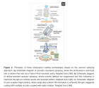
Mechanisms of Film-Formation-Related Defects in EUV Photoresists for Sub-3 nm Nodes and Synergistic Materials–Process–Intelligence Co-Optimization​

Abstract​

With the advancement of High-NA EUV lithography and the continued evolution of transistor architectures toward GAA and CFET, semiconductor manufacturing has entered the sub-3 nm technology node era. At advanced nodes, photon shot noise becomes increasingly significant, while the process tolerance window narrows substantially. Photoresist film-formation-related defects may originate from multiple stages of the fabrication process, including coating, exposure, post-exposure bake, development, and etching/stripping, and are strongly influenced by microscopic stochastic effects. However, the isolated optimization of materials, processes, or intelligent control strategies still suffers from significant limitations. Therefore, this review systematically examines the formation mechanisms and cross-process evolution of photoresist film-formation-related defects within the development trajectory of advanced lithography. An integrated materials–process–intelligence co-optimization framework is proposed to elucidate the coupling mechanisms among these three dimensions and the construction of a full-chain closed-loop control strategy. The current challenges and future development directions are summarized, providing optimization insights for both academic research and industrial implementation. This review aims to establish a defect-control framework integrating fundamental understanding with engineering considerations, thereby supporting low defectivity, high robustness, and improved manufacturability for sub-3 nm node patterning.​

1784663907255.png

Please, Log in or Register to view URLs content!
 

tokenanalyst

Lieutenant General
Registered Member

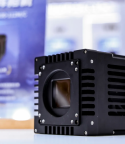
ECO Optoelectronics Showcased Full Range High End Visual Sensors For Semiconductor Inspection​


ECO Optoelectronics showcased its full range of high-end imaging products at this year's Vision China, focusing on cutting-edge applications in precision manufacturing industries such as semiconductors, 3C electronics manufacturing, and new energy, demonstrating its technological accumulation and innovative leadership in the field of industrial sensing.

Semiconductor Industry - Precision Testing at the Chip Level

Focusing on the pain points of semiconductor process inspection, ECO Optoelectronics provides a precise sensing solution across the entire chain, breaking down technical barriers and achieving precise sensing at the chip level.

105MP high-speed area scan camera

Equipped with a 100Gbps CoF interface and an ultra-high frame rate of 112fps, it achieves high-speed, real-time, and latency-free transmission, meeting the high-speed and precision testing requirements in semiconductor manufacturing processes.

SG4050 Linear Spectral Confocal Sensor

With an ultra-large measurement field of view of 20.4mm and a scanning speed of 18kHz, its technical specifications reach the international advanced level, improving the accuracy and efficiency of semiconductor packaging processes.

8K High-End TDI Linear Scan Camera

With an ultra-high line frequency of 1000kHz for improved efficiency and speed, and upgraded sensitivity in the ultraviolet band, it can accurately capture wafer surface defects even in low light.

Intelligent focusing system

It supports a 66mm target surface with a wide field of view and 6.3kHz high-speed defocus sampling, easily meeting the high-speed real-time focusing needs of complex textures on the surface of wafers with images.

1784664454033.png1784664492328.png

Please, Log in or Register to view URLs content!
 

tokenanalyst

Lieutenant General
Registered Member

The Institute of Microelectronics has made significant progress in the field of 3D simulation of DRAM etching processes.​

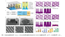
As DRAM manufacturing processes continue to shrink, controlling the etching morphology of the active region fin structure has become a key bottleneck for improving yield. The industry has widely observed the wiggling AA effect, where non-uniform sidewalls and bending distortion appear in the fin structure, severely reducing capacitance efficiency and device reliability. However, its physical root cause has long been unclear, lacking systematic characterization and mechanistic models, making it difficult to precisely control the etching process.

To address the aforementioned challenges, Researcher Rui Chen from the EDA Center of the Institute of Microelectronics, Chinese Academy of Sciences, in collaboration with Senior Engineer Junjie Li and Senior Engineer Jing Wen from the Pilot Center, and Professor Lado Filipovic from the Vienna University of Technology, innovatively integrated focused ion beam scanning electron microscopy (FIB-SEM) three-dimensional reconstruction technology with etching process models. By combining simulations and experiments of the etching process under different process conditions, they revealed the core mechanism and regulation mechanism of the wiggling AA effect.

The research findings were recently published in Communications Engineering, a sub-journal of Nature's engineering field, entitled "3D reconstruction and etching profile simulation for wiggling active area effect in dynamic random access memory manufacturing." Ziyi Hu, a doctoral student at the Institute of Microelectronics, is the first author of the paper, and Rui Chen, a researcher at the Institute of Microelectronics, Junjie Li, a senior engineer, and Professor Lado Filipovic of the Vienna University of Technology are the co-corresponding authors. This research was supported by the National Key Research and Development Program of China (Young Scientists Program), the National Natural Science Foundation of China (General Program), and the International Partnership Program of the Chinese Academy of Sciences.

1784670112576.png
Please, Log in or Register to view URLs content!
 

tokenanalyst

Lieutenant General
Registered Member

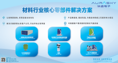
Huacheng Electronics showcases its core components at FINE 2026​


From June 10th to 12th, the 2026 Future Industry New Materials Conference ( FINE 2026 ) was grandly held in Shanghai. The exhibition focused on five core areas: advanced semiconductors, advanced batteries, lightweighting, low-carbon sustainability, and thermal management, creating a full-chain innovation display and cooperation platform encompassing "cutting-edge technology new materials core components end-end applications." Huacheng Electronics sincerely thanks every industry colleague who visited our booth to join us in this future industry innovation feast and explore new opportunities for the synergistic development of new materials and precision components.

At this exhibition, Huacheng Electronics showcased its core component products for the carbon materials industry, covering a range of products including RF power supplies, gas mass flow controllers, gas pressure controllers , and miniature vacuum gauges. Currently, Huacheng Electronics' products and solutions have gained recognition from numerous customers, holding a significant market share in the diamond culture industry.

1784670835933.png

Please, Log in or Register to view URLs content!
 

tokenanalyst

Lieutenant General
Registered Member

Academician Zhang Jin's team at Peking University breaks through the bottleneck of carbon nanotube diameter control.​


Academician Zhang Jin’s team at Peking University has successfully overcome a major bottleneck in carbon nanotube (CNT) technology: precise control over tube diameter while maintaining high-quality, high-density horizontal array growth. This achievement was published in the Journal of the American Chemical Society on July 20, 2026.

Traditional silicon semiconductors are approaching their physical limits, making CNTs a promising alternative due to their high carrier mobility and nanoscale structure. However, the electrical properties of CNTs depend heavily on their diameter, which determines the band gap; for future 3 nm technology nodes, CNTs need a diameter of approximately 1.3 nm to ensure low leakage and high performance. Existing methods have struggled to control catalyst particle size which dictates CNT diameter without causing agglomeration, reducing array density, or damaging alignment, creating a significant barrier to practical application.

To address this, the team developed a novel interface engineering strategy called "sulfur-modified sapphire" (S-apphire). By modifying the sapphire substrate surface with sulfur, they altered the interaction between the metal catalyst and the substrate. They used cohesive energy (EcohEcoh) as a key descriptor to regulate catalyst particle size, a method that allows for precise diameter adjustment without changing the catalyst system or damaging the substrate crystal structure.

Experimental results showed that in Titanium (Ti) catalytic systems, the average CNT diameter was reduced from 1.57 nm to 1.26 nm, closely matching the requirements for 3 nm node transistors. Importantly, the modified CNTs retained high growth density, excellent orientation, and low defect levels. Field-effect transistors fabricated using these 1.26 nm CNTs achieved an on/off ratio of nearly 107107, representing an improvement of almost two orders of magnitude compared to non-optimized devices (~105105).

This breakthrough provides a crucial material foundation for high-performance carbon-based integrated circuits and offers a new general strategy for catalyst design and nanomaterial control using cohesive energy as a descriptor. It reinforces carbon nanotubes as a viable candidate for semiconductor technology in the post-Moore era, despite remaining challenges in wafer-level manufacturing and purity control.​


Please, Log in or Register to view URLs content!
 

tokenanalyst

Lieutenant General
Registered Member

MOCVD equipment company Blue River Technology completes hundreds of millions of yuan in Series B6 financing.​


Lanhe Technology (Shaoxing) Co., Ltd., a prominent manufacturer of MOCVD (Metal Organic Chemical Vapor Deposition) equipment, has successfully completed its B6 financing round, raising hundreds of millions of RMB. The investment was led by the China Internet Investment Fund, with participation from institutions such as Taida Sci-Tech Innovation and Changjiang Innovation. This latest funding milestone underscores the strong support Lanhe Technology continues to receive from both industrial and financial investors, significantly bolstering the domestication process of core equipment for compound semiconductors in China.

MOCVD technology is critical for the epitaxial growth required in manufacturing compound semiconductors, which are essential for high-end devices like optical communication chips, power semiconductors, and space photovoltaic cells. Historically, the global high-end MOCVD market has been dominated by a duopoly of Germany's Aixtron and America's Veeco, leaving China with a localization rate of less than 10% in advanced applications such as GaN power devices. As the only domestic company achieving mass shipments across a full material system, Lanhe Technology has built a comprehensive equipment platform covering second-generation (InP/GaAs), third-generation (GaN/SiC), fourth-generation (Ga₂O₃, AlN), and two-dimensional thin-film materials, serving over 50 industrial clients and 40 research institutes with more than 150 units shipped.
1784733676349.png
1784733700567.png

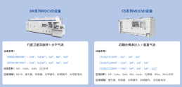
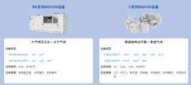
The current surge in demand for domestic MOCVD equipment is primarily driven by breakthroughs in optical communications and space photovoltaics. Lanhe Technology’s DR and CS series equipment have been widely adopted by leading industry players in optical communications, while its GaAs-based space photovoltaic MOCVD systems are seeing bulk shipments to support the low-orbit satellite internet sector. The newly raised funds will be strategically allocated to core process iterations, capacity expansion, and R&D team growth, aiming to accelerate industrial verification and mass delivery of various equipment models, thereby breaking foreign monopolies and enhancing the autonomy and security of China’s compound semiconductor supply chain.​

Please, Log in or Register to view URLs content!
 

tokenanalyst

Lieutenant General
Registered Member
Molybdenum targets are also used in the coating of EUV mirrors.​

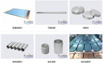
Fenglianke Optoelectronics Begins Mass Production and Shipment of G8.7 AMOLED Core Materials


Fenglianke Optoelectronics (Luoyang) Co., Ltd., a subsidiary of Longhua Technology Group, has successfully completed final testing, packaging, and shipment of its G8.7 AMOLED-specific silver alloy sputtering targets. This marks the start of mass production for this critical display material.

The company now possesses completely independent intellectual property rights for this product, joining a select group of global companies that have mastered its mass production technology. This achievement fills a gap in China's upstream materials supply for high-generation flexible displays, supporting domestic substitution and reducing reliance on foreign suppliers. The target material's microstructure uniformity and density have reached internationally advanced levels, with performance comparable to overseas competitors.

Founded in 2001, Fenglianke specializes in high-end sputtering targets. It supplies core materials (including high-purity molybdenum, silver alloy, and ITO targets) to major global panel manufacturers such as BOE, Tianma, TCL CSOT, Visionox, LGD, and Samsung. The company has achieved 100% self-sufficiency in the entire production chain for G8.7 silver alloy targets through innovations in alloy formulation, vacuum melting, large-size molding, and precision processing. This development strengthens China's new display industry chain, particularly supporting the growth of flexible OLED, foldable screens, and high-end smart displays.

1784734232755.png

Please, Log in or Register to view URLs content!
 
Top