Chinese semiconductor thread II

tokenanalyst

Lieutenant General
Registered Member

Jingce Electronics continues to support the high-quality development of the automotive electronics testing industry with its innovative achievements.​


Jingce Electronics has made a strong international debut with its innovative technological achievements, showcasing three main products on the European international stage: the cockpit domain controller testing system, the cockpit domain controller aging test system, and the automotive electronics testing connector product series. With optoelectronic testing equipment and scenario solutions, Jingce Electronics helps global intelligent vehicle industry customers achieve full-process quality control and yield management from R&D to mass production.

As a leading service provider of automotive electronic testing solutions in the industry, Jingce has made a powerful overseas debut on the European international stage with its innovative technological achievements. Jingce showcased three core product lines, including cockpit domain controller test system, cockpit domain controller aging test system, and automotive electronic test connector product series. Leveraging optoelectronic inspection equipment and scenario-based solutions to support global intelligent vehicle manufacturers in full-process quality control and yield management covering the entire chain from R&D to mass production.

Jingce Electronics focuses on the mass production testing needs of automotive intelligent cockpit domain controllers and has launched a cockpit domain controller testing system. It is fully compatible with mainstream automotive chip platforms and provides one-stop coverage for all dimensions of testing needs, including power management, vehicle communication, audio and video links, radio frequency, and domain control integration . It has already been deployed in batches on the mass production lines of several leading Tier 1 customers.

Jingce focuses on the end-of-line testing demands for mass-produced automotive cockpit domain controllers, has launched cockpit domain controller test system. Fully compatible with mainstream automotive chip platforms, It delivers one-stop testing coverage cross all dimensions including power management, vehicle-mounted communication, audio and video links, radio frequency and domain control of mainstream chip platforms. The system has already been deployed in volume on mass production lines of multiple leading Tier 1 customers.
1784230958795.png1784230980457.png
Please, Log in or Register to view URLs content!
 

tokenanalyst

Lieutenant General
Registered Member

Xiamen University and Huawei jointly announced a new achievement: heterogeneous integration of 4-inch diamond wafers.​


Xiamen University, in collaboration with Huawei Technologies and Xiamen Yuntian Semiconductor, announced a significant advancement in chip thermal management. The research, published at the 2026 IEEE 76th Electronic Components and Technology Conference (ECTC), addresses the critical challenge of heat dissipation in high-performance chips used in 5G, AI, and automotive electronics.

As chip power consumption exceeds 1000W, traditional cooling methods are reaching their limits. Diamond, with its ultra-high thermal conductivity (>2000 W/(m·K)), is an ideal candidate for next-generation cooling, but integrating it with silicon semiconductors has been difficult due to issues like high interface thermal resistance and wafer warpage.

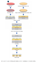
The team developed a 4-inch silicon/diamond wafer-level collective bonding solution. Key technical steps included:​
  • Using temporary bonding to support the diamond wafer, reducing warpage by approximately 67%.​
  • Depositing reactive metal nanolayers after surface plasma activation.​
  • Achieving wafer-level bonding at a low temperature of 200°C.​
Performance Results:
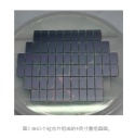
  • Successfully bonded 65 silicon dies to a single 4-inch polycrystalline diamond wafer.​
  • Achieved an extremely low void rate of only 0.31% at the interface.​
  • Reached a minimum thermal boundary resistance of 20.3 m²·K/GW, outperforming many existing bonding methods.​
The integrated samples passed rigorous reliability tests, including 1,000 hours of storage at 150°C, six reflow soldering cycles at 260°C, and 1,050 thermal cycles between -55°C and 125°C.

This study provides a scalable, low-temperature manufacturing path for integrating diamond heat spreaders into advanced packaging. It marks a significant step toward moving diamond thermal materials from laboratory verification to industrial-scale application, offering a promising solution for thermal management in future high-power, high-density chips.​

1784231402976.png1784231516210.png

Please, Log in or Register to view URLs content!
 

gaussgun

New Member
Registered Member

CXMT's DDR5 RAM isn't as performant or as consistent as SK hynix dies, early testing shows — reveals resistance to voltage scaling and inferior manual overclocking capabilities​


Please, Log in or Register to view URLs content!

>Different batches of CXMT-equipped memory perform differently, too, so silicon lottery plays a much bigger role than it would with other vendors.

Probably needs a bit more time
 

Hitomi

Junior Member
Registered Member

CXMT's DDR5 RAM isn't as performant or as consistent as SK hynix dies, early testing shows — reveals resistance to voltage scaling and inferior manual overclocking capabilities​


Please, Log in or Register to view URLs content!

>Different batches of CXMT-equipped memory perform differently, too, so silicon lottery plays a much bigger role than it would with other vendors.

Probably needs a bit more time
Not many do this amount of fine tuning on their RAM in the consumer space, most play around with their GPUs and CPU clocks followed by their cooling. RAM fine tuning is really far down the list of things to fine tune lol.

Not to mention the fine tunes still impact the CXMT RAM, just that the article only stated that it's not as much as the big 3 and he doesn't really go into the numbers, so at that point it might be single percentages that are imperceptible to the average and even the hardcore gamers and only really noticeable when you are running an AI data centre.
 
Last edited:

tokenanalyst

Lieutenant General
Registered Member

Jingsheng Electronics' subsidiary signed a sales contract for semiconductor front-end metrology testing equipment worth approximately 223 million yuan.​


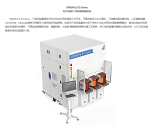
On July 16, Jingce Electronics issued an announcement stating that its holding subsidiary, Shanghai Jingce Semiconductor Technology Co., Ltd., recently signed a sales contract with a customer to sell semiconductor front-end metrology testing equipment such as film thickness series products and OCD equipment. The total contract amount reached RMB 223,062,000.

1784300120624.png

As of the date of this announcement, Shanghai Jingce has signed multiple sales contracts with this customer and its related companies within the past twelve months, with a total contract value of RMB 329,752,080 (including this contract).

According to the announcement, the main subject of the contract is semiconductor front-end metrology testing equipment, etc. The contract will become effective upon being sealed or signed by both parties, and delivery will be arranged within 3 to 6 months after the order becomes effective. This contract signing is a routine business activity of the company and does not constitute a related-party transaction, nor does it constitute a major asset restructuring as defined in the "Measures for the Administration of Major Asset Restructuring of Listed Companies."

Because some information in the contract involves trade secrets, Jingce Electronics has exempted itself from disclosing specific customer information in accordance with relevant regulations. The company stated that the customer has good credit, the ability to perform the contract, and the performance risk is controllable, and there is no affiliation between the customer and the company.

Jingce Electronics stated that if this contract is successfully fulfilled, it is expected to have a positive impact on the company's operating results. The signing of this contract further deepens the cooperative relationship between the company and the client, building upon their existing strong partnership. It reflects the client's high regard for the company's semiconductor quality inspection equipment and will help expand the company's brand influence and enhance its market competitiveness. Furthermore, the performance of this contract will not affect the company's business independence, and the company's main business will not become dependent on the party involved as a result of fulfilling the contract.

Please, Log in or Register to view URLs content!
 

tokenanalyst

Lieutenant General
Registered Member

Fudan Microelectronics Unveils Strategic New Products, Marking a Shift to Scenario-Optimized FPGA Solutions


On July 16, Fudan Microelectronics Group held its 28th-anniversary strategic new product launch in Shanghai under the theme "Chips Go Far, Intelligence Creates the Future." The event marked a significant strategic pivot for the company, transitioning from a general chip supplier to a provider of personalized, adaptive computing infrastructure through its new "Scenario-Optimized FPGA" strategy.

The Fudan University Integrated Circuit Engineering Technology Fusion Innovation Center was officially unveiled. Jointly built by Fudan University, Shanghai Guosheng Group, and Fudan Microelectronics, it focuses on next-generation high-end FPGAs, PSoCs, AI, and storage technologies to bridge academic research and industrial application. The company outlined a strategy centered on the "Agent Era," where computing gains autonomy and evolutionary capabilities.

Fudan Microelectronics released a full matrix of products covering three main directions:
  • Edge AI (FMZQ400TAI): A flagship chip based on FPAI heterogeneous fusion architecture using domestic FinFET process. It integrates an 8-core CPU, NPU, and large-capacity FPGA, delivering 128 TOPS@INT8 AI compute power. It supports zero-copy data interaction via unified DDR memory and can form clusters up to 2048 TOPS for deploying large language models (70B parameters) locally.​
  • Communication Side (RFSoC Series 68DR/52DR): These chips integrate RF front-end, ADC/DAC, baseband accelerators, and protocol stacks into a single chip. They offer software-defined radio solutions that reduce system power by 40%, PCB area by 60%, and BOM costs by 30%.​
  • Application Side & IP Ecosystem:
    • Released system-level solutions for commercial aerospace, including satellite autonomous obstacle avoidance and onboard communication payloads.​
    • Launched a comprehensive IP ecosystem covering AI inference/training, scientific computing, post-quantum cryptography, video codecs, and signal processing.​
  1. Fathom L4 Agent Intelligent FPGA Development Platform:
    • To address the complexity of FPGA development, Fudan Microelectronics introduced Fathom L4 Agent. This platform automates the entire FPGA development lifecycle (from requirements to deployment) using AI agents.​
    • It aims to transform engineers from code writers to architectural decision-makers, having already supported over 100 projects and saving thousands of engineering hours.​
This launch signifies Fudan Microelectronics' upgrade to a holistic solution provider encompassing chips, computing power, system solutions, and Agent digital employee services. By leveraging its academic roots and focusing on autonomous innovation, the company aims to empower various industries from healthcare and finance to aerospace with adaptive, intelligent computing infrastructure.​

Please, Log in or Register to view URLs content!
 
Top