You are using an out of date browser. It may not display this or other websites correctly.
You should upgrade or use an alternative browser.
You should upgrade or use an alternative browser.
Chinese semiconductor thread II
- Thread starter vincent
- Start date


Interesting
Suzhou EUV Semiconductor Unveils Breakthrough Three-Beam DPP-EUV Light Source Prototype to Bypass ASML Patents & Accelerate Domestic Lithography
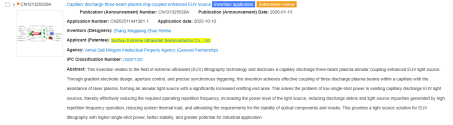
Suzhou Extreme Ultraviolet Semiconductor Co., Ltd. has officially released an engineering prototype of its self-developed three-beam plasma-coupled Discharge-Produced Plasma (DPP) EUV (13.5nm) light source. Led by Dr. Zhang Xingqiang and his team from Harbin Institute of Technology, the innovation offers a fully autonomous, low-cost alternative to ASML’s dominant Laser-Produced Plasma (LPP) route, while solving long-standing industrialization bottlenecks of traditional single-beam DPP systems.
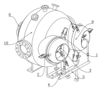
Global commercial EUV lithography relies on LPP technology, which faces heavy patent walls, requires expensive high-power CO₂ lasers, and suffers from severe debris contamination at 50kHz operation rates. Traditional single-beam DPP sources struggle with low power output, rapid electrode degradation, and poor beam stability. The new prototype circumvents these issues by using gradient electrodes and a nanosecond synchronization system to merge three independent capillary plasmas into a large ring-shaped emission zone, fundamentally improving efficiency and scalability.
Global commercial EUV lithography relies on LPP technology, which faces heavy patent walls, requires expensive high-power CO₂ lasers, and suffers from severe debris contamination at 50kHz operation rates. Traditional single-beam DPP sources struggle with low power output, rapid electrode degradation, and poor beam stability. The new prototype circumvents these issues by using gradient electrodes and a nanosecond synchronization system to merge three independent capillary plasmas into a large ring-shaped emission zone, fundamentally improving efficiency and scalability.
- High Power at Low Frequency: Achieves 630–1,050W of industrial-grade power at only 600–1,000Hz, drastically cutting thermal load and cooling requirements.
- Superior Beam Quality & Stability: Ring-shaped emission area improves photon collection efficiency and meets strict ±0.3% energy stability standards required for chip manufacturing.
- Low Debris & Long Lifespan: Reduced plasma frequency minimizes target ablation and optical mirror contamination, extending component life to over 1 year of continuous operation.
- Fully Domestic Supply Chain: Eliminates reliance on foreign lasers and precision parts; core components (capillaries, pulsed power supplies, vacuum modules, xenon gas systems) are fully locally producible.
- IP Independence: Entire architecture is original, bypassing overseas LPP patent blocks and enabling rapid commercial deployment.
The company has outlined a three-phase rollout: short-term aging tests and debris-suppression optimization; mid-term collaboration with Chinese suppliers to assemble an EUV lithography prototype; and long-term development of a fully autonomous commercial EUV system. Industry analysts note that this DPP-based pathway diversifies China’s EUV strategy, significantly lowering R&D costs and patent barriers while accelerating the localization of advanced semiconductor manufacturing equipment.
Last edited:

China's first EUV machine is also traditional LPP powered light source just like ASML. but we should have many options like this one. glad Chinese institutes keep pushing the boundaries of different EUV light source.Interesting
Suzhou EUV Semiconductor Unveils Breakthrough Three-Beam DPP-EUV Light Source Prototype to Bypass ASML Patents & Accelerate Domestic LithographySuzhou Extreme Ultraviolet Semiconductor Co., Ltd. has officially released an engineering prototype of its self-developed three-beam plasma-coupled Discharge-Produced Plasma (DPP) EUV (13.5nm) light source. Led by Dr. Zhang Xingqiang and his team from Harbin Institute of Technology, the innovation offers a fully autonomous, low-cost alternative to ASML’s dominant Laser-Produced Plasma (LPP) route, while solving long-standing industrialization bottlenecks of traditional single-beam DPP systems.
Global commercial EUV lithography relies on LPP technology, which faces heavy patent walls, requires expensive high-power CO₂ lasers, and suffers from severe debris contamination at 50kHz operation rates. Traditional single-beam DPP sources struggle with low power output, rapid electrode degradation, and poor beam stability. The new prototype circumvents these issues by using gradient electrodes and a nanosecond synchronization system to merge three independent capillary plasmas into a large ring-shaped emission zone, fundamentally improving efficiency and scalability.View attachment 178291
The company has outlined a three-phase rollout: short-term aging tests and debris-suppression optimization; mid-term collaboration with Chinese suppliers to assemble an EUV lithography prototype; and long-term development of a fully autonomous commercial EUV system. Industry analysts note that this DPP-based pathway diversifies China’s EUV strategy, significantly lowering R&D costs and patent barriers while accelerating the localization of advanced semiconductor manufacturing equipment.
HUGE if true.Interesting
Suzhou EUV Semiconductor Unveils Breakthrough Three-Beam DPP-EUV Light Source Prototype to Bypass ASML Patents & Accelerate Domestic LithographySuzhou Extreme Ultraviolet Semiconductor Co., Ltd. has officially released an engineering prototype of its self-developed three-beam plasma-coupled Discharge-Produced Plasma (DPP) EUV (13.5nm) light source. Led by Dr. Zhang Xingqiang and his team from Harbin Institute of Technology, the innovation offers a fully autonomous, low-cost alternative to ASML’s dominant Laser-Produced Plasma (LPP) route, while solving long-standing industrialization bottlenecks of traditional single-beam DPP systems.
Global commercial EUV lithography relies on LPP technology, which faces heavy patent walls, requires expensive high-power CO₂ lasers, and suffers from severe debris contamination at 50kHz operation rates. Traditional single-beam DPP sources struggle with low power output, rapid electrode degradation, and poor beam stability. The new prototype circumvents these issues by using gradient electrodes and a nanosecond synchronization system to merge three independent capillary plasmas into a large ring-shaped emission zone, fundamentally improving efficiency and scalability.View attachment 178291
The company has outlined a three-phase rollout: short-term aging tests and debris-suppression optimization; mid-term collaboration with Chinese suppliers to assemble an EUV lithography prototype; and long-term development of a fully autonomous commercial EUV system. Industry analysts note that this DPP-based pathway diversifies China’s EUV strategy, significantly lowering R&D costs and patent barriers while accelerating the localization of advanced semiconductor manufacturing equipment.
Because is low cost and high power open the doors for more companies to try. Also helps the domestic EUV inspection equipment industry.China's first EUV machine is also traditional LPP powered light source just like ASML. but we should have many options like this one. glad Chinese institutes keep pushing the boundaries of different EUV light source.
Personally I think similar from the transition from mercury lamps to excimer lasers the industry will move from plasma sources to compact Free Electron Lasers
Polyhe Materials Shanghai Semiconductor Industrial Base Commences Construction
On July 16, 2026, Juhe Group officially launched its semiconductor strategy and the co-construction of its Shanghai headquarters at a ceremony held in Xinzhuang Industrial Zone, Minhang District, Shanghai. During the event, Delanju Semiconductor, a subsidiary under the STAR Market-listed Juhe Materials, broke ground on its semiconductor electronic materials R&D and industrialization project. This milestone marks the full implementation of the company’s "second growth curve" in semiconductor materials across the core industrial hub of the Yangtze River Delta (YRD).
The project will follow a phased investment model, with an initial construction budget of 1.1 billion RMB. According to long-term planning, total cumulative investments are expected to exceed 5 billion RMB. Leveraging Minhang District’s advanced innovation infrastructure and dense cluster of upstream and downstream integrated circuit enterprises, the base will function as an integrated industrial platform covering the full spectrum of semiconductor electronic materials from research and development and pilot manufacturing to large-scale commercial production. It is designed to address regional capacity gaps in high-end domestic semiconductor material manufacturing and strengthen the YRD’s overall IC supply chain ecosystem.
As a nationally designated "single champion" enterprise in China’s advanced new materials sector, Juhe Materials has built an integrated industrial chain spanning powders, pastes, and colloids, positioning it among industry leaders in both technological capability and operational scale. Financial data from 2025 indicates annual revenue of 14.593 billion RMB and net profit attributable to shareholders of 420 million RMB. With 361 self-developed patents, the company is well-equipped to deliver customized material solutions for diverse applications across new energy and semiconductor markets, supported by a stable and robust financial foundation.
Aligned with national priorities for high-quality development in China’s IC sector, Juhe Materials is focusing its technical breakthroughs on achieving supply chain self-reliance. Key R&D tracks include photomasks and photoresists high-end electronic materials historically reliant on foreign suppliers. By establishing its Shanghai complex in Xinzhuang Industrial Zone, the company will be strategically positioned to collaborate closely with leading YRD-based chip designers, semiconductor foundries, and packaging/testing firms. This geographic advantage will significantly shorten product validation cycles, accelerate the mass adoption of domestic new materials across supply chains, and drive large-scale commercialization of indigenous semiconductor technologies, thereby enhancing the security and resilience of China’s integrated circuit industry.
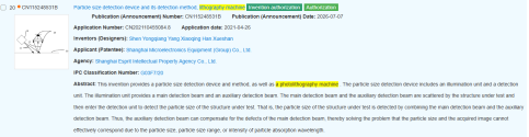
Illumination coherence-controlled power-spectral-density of roughness-induced scattering determines the detectability of phase defects in EUV lithography.
Changchun University Science and Technology
Abstract
Phase-defect inspection is crucial in EUV (Extreme ultraviolet) lithography for achieving high semiconductor-chip yields. While at-wavelength inspection can detect phase defects, inspecting entire masks in a practical timeframe was once a showstopper. This challenge was solved by using a pixel size of 500 nanometers or larger to detect defects tens of nanometers in size. The focus then shifted to reducing the background signal, Rpix, from large pixels. Rpix is greatly reduced in the dark-field configuration and controlling the angular distribution of roughness-induced scattering is essential for defect detection. This paper reports a detailed analysis of the power spectral density (PSD) of surface-roughness-induced scattering using a developed rigorous numerical code. The study concludes that coherence strongly affects PSD, thereby controlling the detectability of phase defects and that the illumination coherence length and the blocking inner numerical aperture NAd are the decisive parameters in the phase-defect inspection.
Huakang Clean jointly won the bid for the Jiufengshan Semiconductor Manufacturing Base Project
Wuhan Huakang Century Clean Technology Co., Ltd. has announced that it successfully won the bid for Section 2 of the Jiufengshan Semiconductor Manufacturing Base Project as part of a consortium led by China Construction Third Engineering Bureau. The engineering procurement construction (EPC) contract is valued at approximately 1.956 billion RMB with an execution period of 730 days, and Huakang Clean’s expected share amounts to roughly 180 million RMB. This award represents a major strategic milestone for the company as it expands from its traditional focus on medical operating room cleanrooms into the high-precision semiconductor fabrication sector.
The transition is driven by the vast market potential in industrial cleanroom applications, which account for over 80% of China’s cleanroom market compared to less than 18% for healthcare facilities. Since launching its electronic semiconductor division in October 2024, Huakang Clean has already secured more than 1.2 billion RMB in orders from leading industry players including AMEC, JCET Group, Goertek, and Lead Intelligent. The company’s bidding volume for electronic cleanrooms this year alone has surpassed its total for the entire previous year, underscoring rapid commercial traction in the new segment.
Delivering semiconductor-grade environments demands significantly higher technical standards than medical facilities, including cleanliness levels as strict as Class 10, nano-level micro-vibration control systems, and integrated delivery platforms for bulk process gases. To meet these requirements, Huakang Clean assembled a specialized engineering team of over 500 professionals capable of designing, integrating, and commissioning 15 complex subsystems. The company has also partnered with more than ten local suppliers, such as Shenglong Electric and Yangtze Electric, to establish a regionalized technical support network. This growth is further reinforced by the mature industrial ecosystem in Wuhan’s Optics Valley, where the integrated circuit industry exceeded 100 billion RMB in output in 2025 and hosts nearly 442 cleanroom-related enterprises covering design, construction, and lifecycle maintenance.