Norelsys is the first chip house in China to design and supply 12G Automotive SerDes chip. It has over 20 chips that meet HSMT standard and covers 2 to 12.8 Gbps, enough to satisfy 15MP camera and 4K@60Hz + 4D MMW radar. It had 17m deliveries by end of 2025.
You are using an out of date browser. It may not display this or other websites correctly.
You should upgrade or use an alternative browser.
You should upgrade or use an alternative browser.
Chinese semiconductor thread II
- Thread starter vincent
- Start date
Numerous links here on the same story of YMTC phase 3 going into production in 2026, just a year after construction started in 2025/9. Its market share is already up to 10%. Huge demand for it in AI, high performance NAND & QLC.
You can see that it's part of Optical valley. 20.7B RMB of registration for this project so far. YMTC controls 50.19% of shares here & 湖北长晟三期 investment fund controls 49.81% share.
Expecting domestic equipment to be 70%+ here vs 50% in phase 2 plant & 30% in phase 1 plant.
YMTC is in Huawei, Xiaomi supply chain. Its industrial SSD is used by Alibaba & Tencent cloud. Order backlog is full until Q2.
Confused, I thought that YMTC was going 100% domestic. Is that a smaller experimental line?
well, there are many production lines in each fab. Each plant will eventually produce 100k wpm. The first all domestic production line is almost assuredly going to be in phase 2 fab.Confused, I thought that YMTC was going 100% domestic. Is that a smaller experimental line?
It's unclear to me whether 50 & 70% are truly going to be accurate since these are all estimates and will depend on how well the all domestic line works out. It is certainly reasonable for them to continue to use some ASML and TEL machines on other lines until the yield all on domestic line rises to the same level.
Hebei Dingci Electronics Initiates IPO Preparation, Focusing on the Localization of High-End Electronic Ceramic Packaging Substrates
Hebei Dingci Electronic Technology Co., Ltd. has officially begun its initial public offering (IPO) process, filing with the China Securities Regulatory Commission (CSRC), marking its entry into the capital market. The company, established in 2015 with a registered capital of 40.77 million yuan, specializes in high-end electronic ceramic packaging substrates and bases—critical components for advanced technologies such as 5G, aerospace, and smart sensors. As a key player in China’s “domestic substitution” initiative, Dingci Electronics has developed a leading domestic production line for multilayer ceramic packaging materials, helping to resolve critical bottlenecks in high-end electronic materials.
Backed by strong R&D capabilities and recognized as a National High-tech Enterprise and a Specialized Innovative SME in Hebei Province, the company’s projects are included in provincial strategic emerging industries plans. The IPO is strategically timed to expand production capacity and accelerate innovation, enabling Dingci Electronics to strengthen its market position and support China’s broader goals of industrial self-reliance and control over critical supply chains.
The national standard adopts 19 SiC/GaN/LED group standards from CASA & CSA
China’s National Standardization Administration formally adopted 19 group standards from two leading industry alliances—CASA and CSA—into its national standardization framework, representing 25% of the 76 standards selected in the first batch of the year. This move underscores the government’s commitment to elevating domestic third-generation semiconductor and LED technologies from industry-led initiatives to nationally recognized benchmarks. The adoption process, with a streamlined six-month cycle, reflects a strategic push to accelerate innovation and standardization in critical high-tech sectors, ensuring consistency, safety, and global competitiveness for Chinese manufacturers.
CASA contributed 13 standards centered on silicon carbide (SiC) and gallium nitride (GaN) power devices, covering essential reliability and performance testing protocols. These include seven advanced SiC MOSFET stress tests—such as high-temperature reverse bias (HTRB) and dynamic high-temperature humidity reverse bias (DH3TRB)—alongside three standards for dynamic parameters like gate charge and switching behavior. Additionally, three GaN-specific standards address critical applications in 5G infrastructure, including test methods for Sub-6GHz power amplifier modules and specifications for silicon-substrate GaN epitaxial wafers, positioning China at the forefront of next-generation power electronics and wireless communications.
Meanwhile, CSA’s six adopted standards focus on practical, high-impact LED applications, spanning UV disinfection, lighting design, and niche commercial uses. These include performance criteria for UVA photocatalysis modules, mosquito-attracting lamps, and deep-UV packaging reliability, as well as technical guidelines for phosphorless multi-color LED lighting, landscape illumination control, and LED fish-attracting lamps for fishing vessels. By formalizing these standards, China not only enhances product quality and consumer safety but also creates a scalable framework for emerging LED markets, reinforcing its leadership in both semiconductor materials and smart lighting technologies.
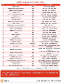
where are key players like Piotech and Skyverse ?? both firms had record revenue last year.SMEE is ahead of ShengMei, so revenue at least 8 billion rmb. What did he sell?
View attachment 169052
but yeah the interesting thing is, SMEE revenue which stated 7+ Billion RMB. they also mentioned 28nm scanner. @tokenanalyst bro your analysis.
Tianjin's first early-stage integrated circuit special fund was officially launched.
On January 30, 2026, Tianjin launched its first early-stage integrated circuit (IC) venture fund — the Tianjin Chipfire Integrated Circuit Venture Capital Fund at the 2025 Tianjin IC Industry Association Re-election and Innovation Conference. Managed by Shenzhen Jinghu Capital, the fund has a target size of 200 million yuan and focuses on early-stage investments of 1–10 million yuan in critical IC sectors: semiconductor equipment, EDA tools, high-end chip design, advanced materials, and intelligent sensors.
Co-established by the Tianjin Angel Investment Guidance Fund, Tianjin Binhai High-tech Industry Investment Fund, and private capital, the fund completed registration with the Asset Management Association of China in June 2025 and is now actively investing. At the launch, it signed agreements with five startups for 30 million yuan in commitments.
As Tianjin’s first dedicated early-stage IC fund, it aims to solve startup financing bottlenecks, support domestic substitution in key technologies, and leverage the Tianjin National Chip Spark Innovation and Entrepreneurship Platform to provide integrated “investment + incubation + acceleration” services. This initiative is expected to strengthen Tianjin’s IC ecosystem and boost the broader Beijing-Tianjin-Hebei hard technology cluster.
Simultaneously, the Chip Spark Platform unveiled the “Chip Collaboration Venture Capitalist” program, designed to connect IC scientists with investors and partners through matchmaking events, further nurturing high-potential startups and enhancing regional innovation.
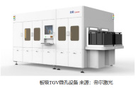
Di'er Laser's export order for panel-grade laser micro-hole equipment has been successfully shipped.
Wuhan Di'er Laser Technology Co., Ltd. has successfully shipped its first export order of panel-level laser micro-hole equipment for glass substrate semiconductor packaging a major breakthrough in advanced semiconductor packaging and a sign of global recognition for its technology.
As Moore’s Law hits physical limits, advanced packaging particularly using glass substrates has emerged as a critical pathway to meet the performance demands of AI and high-performance computing (HPC). Glass substrates offer superior thermal stability, flatness, low thermal expansion, and dielectric properties compared to traditional organic materials, making them ideal for interposers and IC substrates.
At the heart of glass substrate adoption is TGV (Through-Glass Via) technology, which enables vertical electrical connections via micro-vias. Laser processing known for non-contact precision and high efficiency has become the industry standard for TGV fabrication.
Since 2019, Di'er Laser has developed a proprietary one-stop solution combining laser modification, chemical etching, and AOI inspection, achieving industry-leading performance:
- Minimum hole diameter: ≤5µm
- Depth-to-diameter ratio: ≥100:1
- High yield and processing stability across diverse glass materials

This innovation breaks the long-standing monopoly of foreign equipment suppliers. The export of Di'er Laser’s TGV equipment not only marks a milestone for the company but also accelerates the domestic Chinese glass substrate supply chain, enhancing China’s role in the global advanced packaging ecosystem.
With global giants like TSMC, Intel, and Samsung ramping up glass substrate investments, and Chinese firms like BOE and Woguang advancing industrialization, Di'er Laser aims to further refine its laser micro-nano processing tech and collaborate globally to build a complete industry ecosystem.
Looking ahead, glass substrates are poised to replace organic ones in high-end HPC markets, becoming the standard for trillions-of-transistor integration and Di'er Laser is positioned as a key enabler of this transformation.

